Preparation method for surface-enhanced Raman scattering substrate

A surface-enhanced Raman and substrate technology, applied in the directions of Raman scattering, sputtering coating, superimposed layer coating, etc., can solve the problems of insufficient sensitivity and measurement speed, and achieve the effect of enhancing Raman scattering and avoiding oxidation

Active Publication Date: 2018-10-09
HANGZHOU DIANZI UNIVERSTIY INFORMATION ENG SCHOOL
View PDF3 Cites 4 Cited by
  • Summary
  • Abstract
  • Description
  • Claims
  • Application Information

AI Technical Summary

Problems solved by technology

Therefore, SERS technology can be used in trace substance analysis, flow cytometry and other applications, which are not enough for the sensitivity and measurement speed of traditional Raman spectroscopy detection methods

Method used


Image

  • Preparation method for surface-enhanced Raman scattering substrate
  • Preparation method for surface-enhanced Raman scattering substrate
  • Preparation method for surface-enhanced Raman scattering substrate

Examples


preparation example Construction

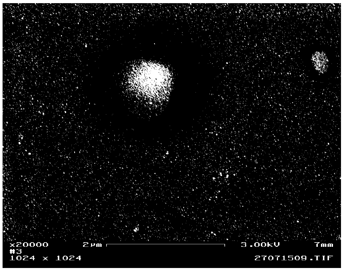
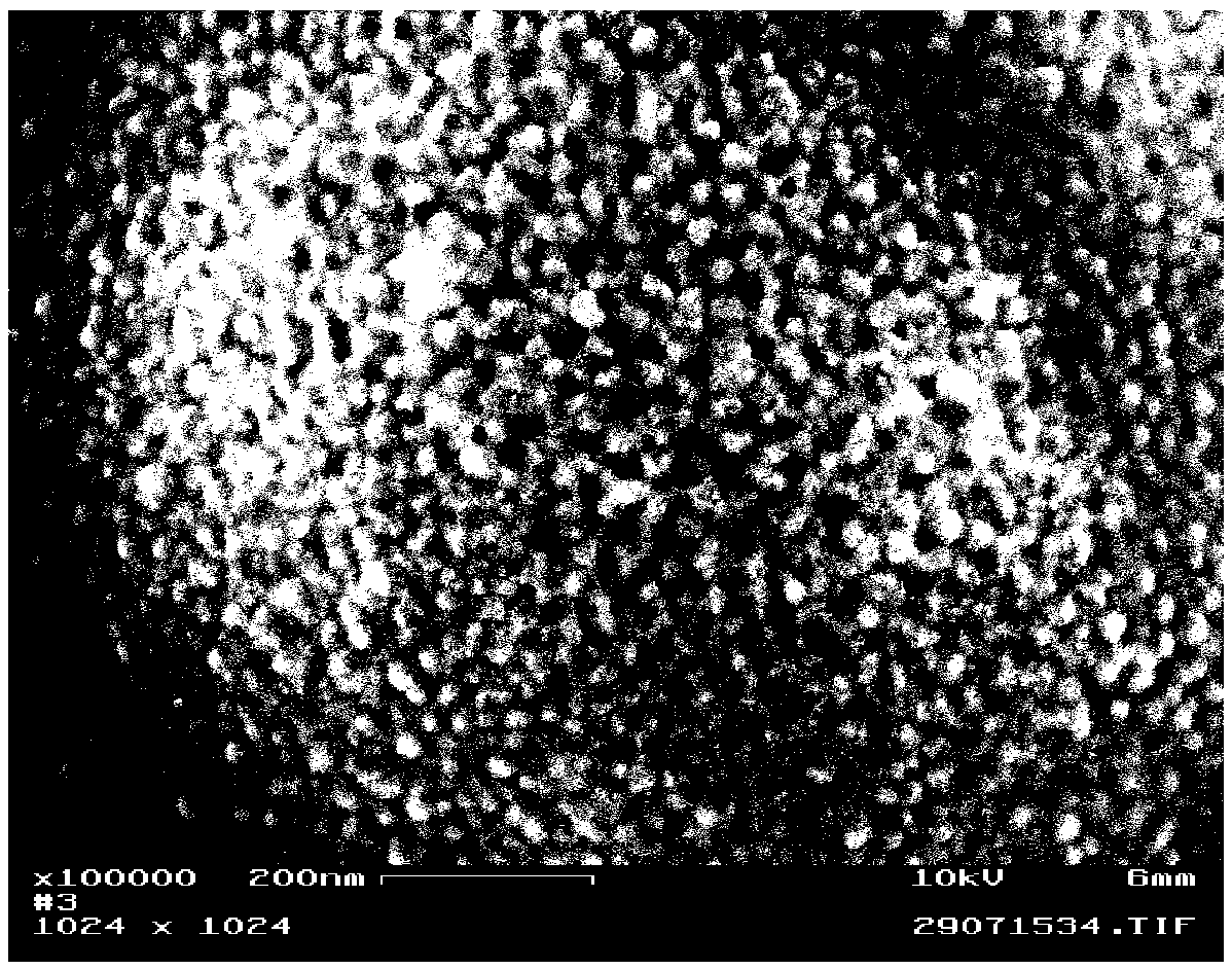
[0031] Such as figure 1 , figure 2 Shown, a kind of preparation method of surface-enhanced Raman scattering substrate specifically comprises the following steps:

[0032] Step 1. The Si(100) substrate used for depositing samples was ultrasonically cleaned for 15 minutes each with detergent, acetone, absolute alcohol and deionized water in sequence, and then set aside.

[0033] Step 2. Place the cleaned Si substrate in CVD, pass through methane, and deposit graphene at high temperature;

[0034] Step 3. Place the substrate deposited with graphene on the sample stage of magnetron sputtering, wherein the first sample stage is empty, and the other three sample stages place the Si substrate; and align the current position of the copper target with the first sample stage. One sample stage; four sample stages and the surface of the copper target are all set in the vacuum chamber, and the sample stage is parallel to the surface of the copper target and the distance is 55mm-60mm; ...

Embodiment 1

[0053] The present invention prepares graphene on Si substrate by CVD, prepares Cu on graphene substrate by magnetron sputtering 3 N thin film, using SEM to expose the sample to an electron beam, finally forming a nanoporous copper structure, thereby completing the preparation of the SERS substrate. First, the substrate used for depositing samples was ultrasonically cleaned for 15 minutes with detergent, acetone, absolute alcohol and deionized water in sequence, and then the substrate was placed in CVD, methane was passed through, and graphene was deposited at high temperature. After that, the substrate deposited with graphene is placed on the sample holder of the magnetron sputtering equipment. The sample holder is parallel to the target surface and 55mm apart. -6 At mbar, feed a mixed gas with a flow rate of 40 sccm into the vacuum chamber, and the flow ratio of the mixed gas nitrogen and argon is 20:1; turn on the radio frequency source, preheat for 5 minutes, turn on the r...

Embodiment 2

[0055] The present invention prepares graphene on Si substrate by CVD, prepares Cu on graphene substrate by magnetron sputtering 3 N thin film, using SEM to expose the sample to an electron beam, finally forming a nanoporous copper structure, thereby completing the preparation of the SERS substrate. First, the substrate used for depositing samples was ultrasonically cleaned for 15 minutes with detergent, acetone, absolute alcohol and deionized water in sequence, and then the substrate was placed in CVD, methane was passed through, and graphene was deposited at high temperature. After that, the substrate deposited with graphene is placed on the sample holder of the magnetron sputtering equipment. The sample holder is parallel to the target surface and 55mm apart. -6 At mbar, feed a mixed gas with a flow rate of 30 sccm into the vacuum chamber, and the flow ratio of the mixed gas nitrogen and argon is 10:1; turn on the radio frequency source, preheat for 10 minutes, turn on the ...


PUM


Abstract

The invention discloses a preparation method for a surface-enhanced Raman scattering substrate. The preparation method comprises the following steps of: firstly cleaning a Si substrate used for depositing a sample; then, putting the substrate into CVD; leading in methane, depositing graphene at a high temperature, putting the substrate into a sample strand of magnetron sputtering equipment, and enabling the sample stand to be parallel to a target surface and enabling the sample strand to be spaced with the target surface by 55 mm; leading in a gas mixture with flow speed being 40 sccm when bottom gas pressure in a vacuum cavity is lower than 6*10<-6> mbar, thereby sputtering a copper target; after sputtering and coating, taking out a Cu3N film sample and putting the Cu3N film sample into an SEM sample room, vacuum-pumping, selecting an electron beam exposure mode, regulating electron beam focusing, controlling beam spots of an electron beam to be about 1 micron, and performing electronbeam exposure on a Cu3N film selected area; and starting an SEM scanning mode to perform SEM image-forming on an exposure area, and observing exposed morphology. The substrate prepared by the methodhas surface-enhanced Raman scattering effect, and has a nano-scale rough surface.

Description

technical field [0001] The invention belongs to the field of substrate preparation, in particular to a method for preparing a surface-enhanced Raman scattering (SERS) substrate. Background technique [0002] When molecules with Raman activity are adsorbed on rough metal surfaces, especially on noble metal surfaces with nanoscale roughness, the Raman scattering signal intensity is greatly enhanced, which is called surface-enhanced Raman scattering effect (SERS effect). [0003] SERS technology overcomes the disadvantage of weak signal inherent in traditional Raman spectroscopy, and can increase the intensity of Raman signal by several orders of magnitude, and its enhancement factor can be as high as 10 14 ~10 16 , enough to detect the Raman signal of a single molecule. Therefore, SERS technology can be used in trace substance analysis, flow cytometry and other applications, which are not enough for the sensitivity and measurement speed of traditional Raman spectroscopy dete...

Claims


Application Information

Patent Timeline
Patent Type & Authority Applications(China)
IPC IPC(8): C23C14/06C23C14/35C23C16/26C23C28/04G01N21/65
CPCC23C14/0021C23C14/0641C23C14/35C23C16/26C23C28/04G01N21/658
Inventor 杜允俞优姝
Owner HANGZHOU DIANZI UNIVERSTIY INFORMATION ENG SCHOOL
Why Eureka
Try Eureka