

GaN heterojunction conductivity modulation field effect transistor
A conductance modulation, field effect transistor technology, applied in circuits, electrical components, semiconductor devices, etc., can solve the problems of weak control, poor performance, reduced device transconductance, etc., and achieve the effect of improving forward characteristics
Inactive Publication Date: 2018-10-12
UNIV OF ELECTRONICS SCI & TECH OF CHINA
View PDF6 Cites 9 Cited by
- Summary
- Abstract
- Description
- Claims
- Application Information
AI Technical Summary
Problems solved by technology
[0006] 2. In recent years, the research work of enhanced GaN HEMT has made great progress, but the threshold voltage of enhanced GaN HEMT is relatively low (mostly less than 1V), and the performance is obviously worse than that of depletion-type HEMT.
[0008] (1) Reducing the Al composition or growing a thin barrier layer reduces the 2DEG concentration in the channel, but increases the parasitic resistance and on-state resistance of the AlGaN / GaN HEMT, so the Al composition and barrier layer thickness can only be limited reduced within the range, the threshold voltages are relatively low
[0009] (2) Growth of p-cap capping layer to achieve enhanced HEMT, but the capping layer weakens the control of the gate to the channel, reduces the transconductance of the device, which is not good for high-frequency work, and P-cap technology will introduce P-N junction When the device is working, a large number of holes will be injected into the channel, which will generate a large gate current, resulting in a series of problems such as threshold voltage hysteresis and reliability reduction.
[0010] (3) Recessed gate etching can effectively deplete the 2DEG concentration under the gate, but recessed gate etching requires precise control of the etching depth and will introduce serious etching damage
[0011] (4) F-based plasma treatment is a very promising method to realize enhanced HEMT, but it will introduce injection damage, threshold voltage hysteresis, and high-voltage operation stability problems
However, this technology cannot completely deplete the two-dimensional electron gas in the channel, and cannot give full play to the withstand voltage advantages of GaN materials. At the same time, the deep energy level traps introduced by impurities such as carbon and iron will cause such as increased on-resistance, decreased output current, Negative effects such as current collapse effect and decreased reaction speed
Method used
View moreImage
Smart ImageViewing Examples

Examples
Embodiment Construction
[0038] The solution of the present invention has been described in detail in the summary of the invention, and will not be repeated here.
Login to View More PUM
 Abstract
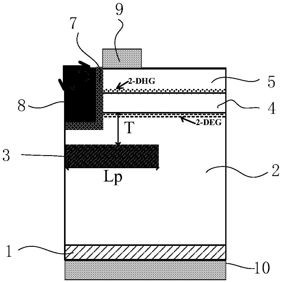
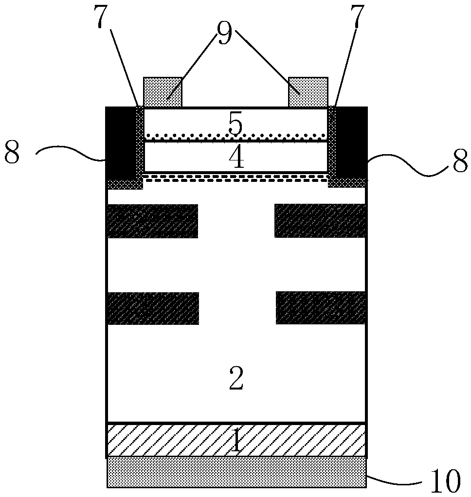
The invention belongs to the technical field of power semiconductors and relates to a GaN heterojunction conductivity modulation field effect transistor. When the GaN heterojunction conductivity modulation field effect transistor is positively switched on, after positive voltage is applied to a drain, a large number of holes are injected into a lightly doped N-type GaN drift region from a P-type heavily doped GaN layer, a large injection phenomenon occurs in the lightly doped N-type GaN drift region, at that same time, a large number of electrons are injected into the drift region from a source electrode for maintaining charge balance, so that the carrier concentration in the orginally lightly doped drift region is increased, the conductivity modulation occurs in the lightly doped N-type GaN drift region, the drift region resistance of the lightly doped N-type GaN drift region is greatly reduced, and the novel structure can further obtain an excellent forward characteristic of low on-resistance and large on-current. During reverse voltage withstanding, a reverse-biased PN junction formed by the floating P-GaN and the N-type drift region is used as gate protection ring to reduce thepeak value of a gate electric field, and a depletion region of the reverse-biased PN junction expands continuously to uniformly distribute the device in the electric field when the reverse-biased PNjunction withstands reverse voltage, so that the reverse leakage current is reduced and the breakdown voltage of the device is increased.
Description
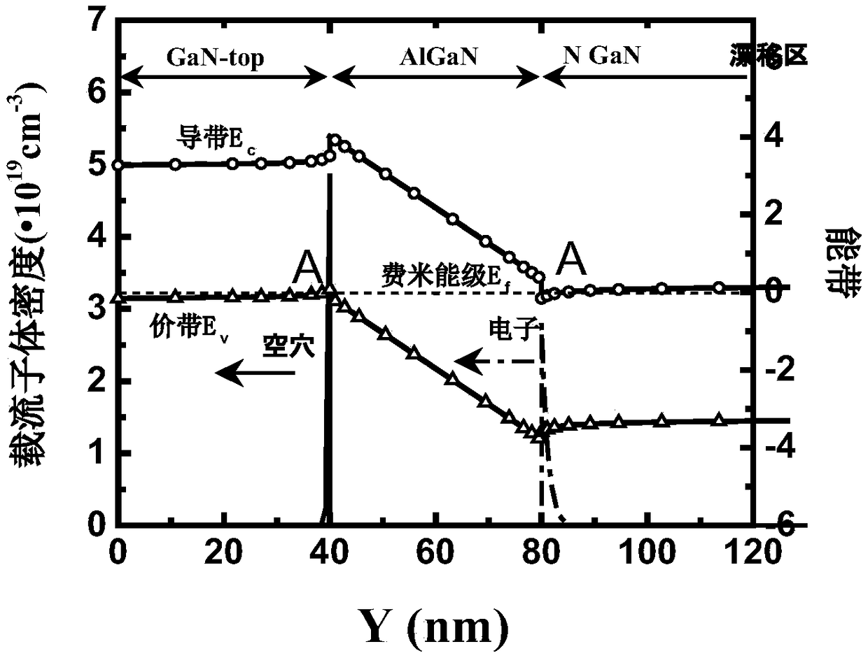
technical field [0001] The invention belongs to the technical field of power semiconductors and relates to a GaN heterojunction conductance modulation field effect transistor. Background technique [0002] Due to the limitations of the first two generations of semiconductor materials represented by Si and GaAs, the third generation of wide bandgap semiconductor materials has been developed rapidly because of its excellent performance. Gallium nitride (GaN) material is one of the cores of the third-generation semiconductor materials. Compared with Si, GaAs and silicon carbide (SiC), the special feature is that it has a polarization effect. Due to the polarization effect of the AlGaN / GaN heterojunction, a two-dimensional electron gas conduction channel with high concentration and high electron mobility is generated at the heterojunction interface close to the GaN side, which makes the AlGaN / GaN HEMT device have small on-resistance and fast switching speed. The characteristics...
Claims
Login to View More Application Information
Patent Timeline
 Patent Type & AuthorityApplications(China)
IPC IPC(8): H01L29/778H01L29/06
CPCH01L29/0684H01L29/7783H01L29/7788
Inventor周琦魏东邓操董长旭黄芃陈万军张波
OwnerUNIV OF ELECTRONICS SCI & TECH OF CHINA