Millimeter wave broadband high efficient transistor stacked power amplifier

A technology of power amplifiers and transistors, applied in power amplifiers, amplifiers with semiconductor devices/discharge tubes, amplifiers, etc., can solve the problems of limited high-power and high-efficiency amplification capabilities, low-cost high-power amplification capabilities, and efficiency indicators. Deterioration and other problems, to achieve the effect of broadband power output capability and power gain capability, good broadband power output capability and power gain capability, and good power and efficiency matching

Pending Publication Date: 2018-10-12
CHENGDU GANIDE TECH
View PDF7 Cites 9 Cited by
  • Summary
  • Abstract
  • Description
  • Claims
  • Application Information

AI Technical Summary

Problems solved by technology

[0004] (1) High-power and high-efficiency amplification capability is limited: With the development of semiconductor technology and the trend of proportional reduction in transistor size, the gate length of transistors is getting shorter and shorter, resulting in a decrease in breakdown voltage and an increase in knee voltage , which limits the output voltage swing of the transistor drain, thereby limiting the power capacity of a single transistor. At the same time, affected by parasitic parameters, the transistor gain of mmWave is also greatly limited
[0005] (2) Low-cost high-power amplification capability is limited: With the development of the third-generation semiconductor process, while the traditional GaAs process maintains the low-cost advantage, it is also necessary to urgently improve the power output capability; and the third-generation semiconductor GaN chip is in The application of millimeter waves is becoming more and more widespread, and there is also an urgent need to reduce costs
[0006] At present, there are many common broadband high-efficiency and high-power amplifier circuit structures, and it is very difficult to meet the requirements of various parameters at the same time. Usually, its high power index will inevitably lead to the deterioration of the efficiency index, while increasing power consumption or chip obtained at the expense of area etc.
[0007] It can be seen from this that the design difficulties of millimeter-wave broadband high-efficiency and high-power amplifiers based on integrated circuit technology are: (1) millimeter-wave ultra-wideband high-power output is more difficult; (2) millimeter-wave high power gain is more difficult; (3) The chip area designed by the traditional millimeter wave method is relatively large

Method used


Image

  • Millimeter wave broadband high efficient transistor stacked power amplifier
  • Millimeter wave broadband high efficient transistor stacked power amplifier

Examples


Embodiment Construction

[0022] Exemplary embodiments of the present invention will now be described in detail with reference to the accompanying drawings. It should be understood that the implementations shown and described in the drawings are only exemplary, intended to explain the principle and spirit of the present invention, rather than limit the scope of the present invention.

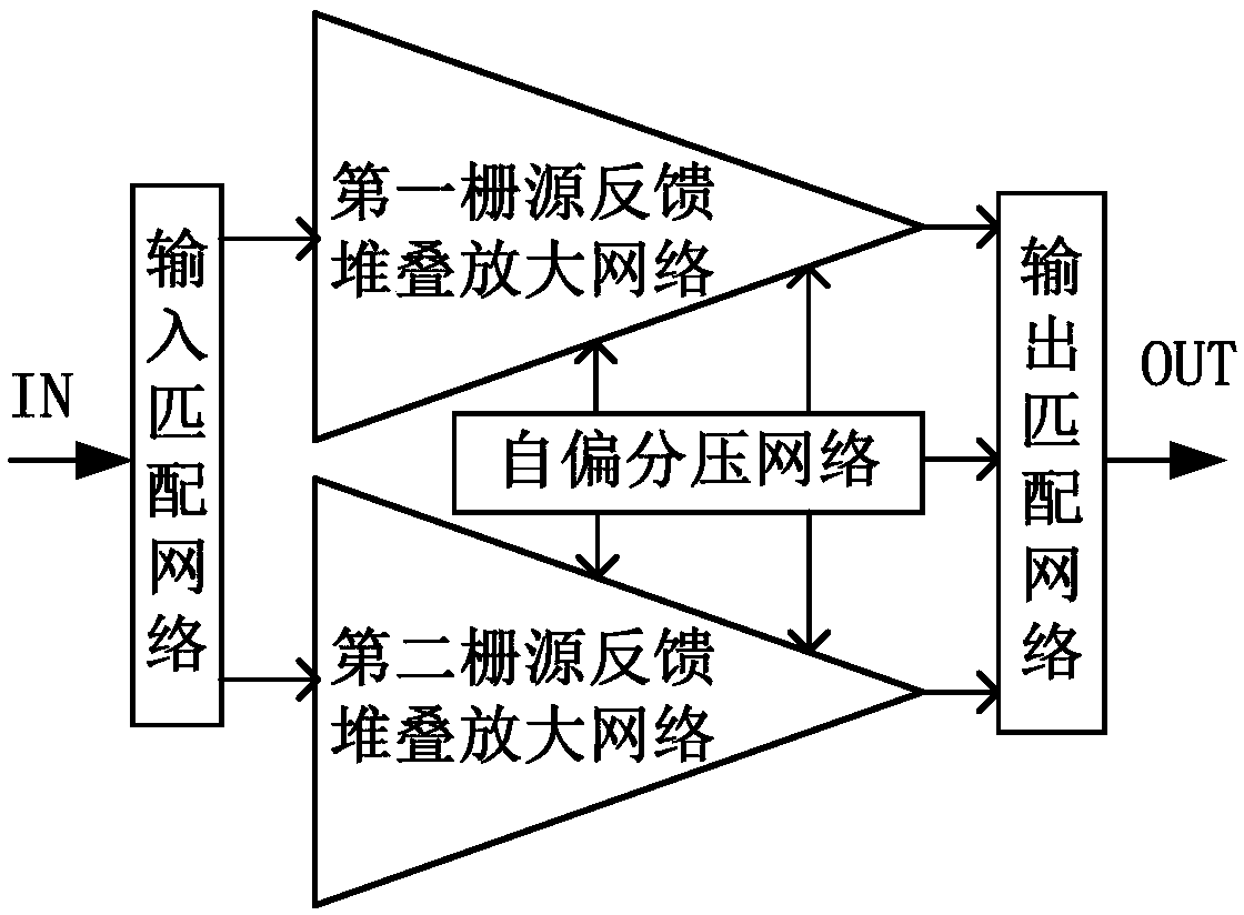
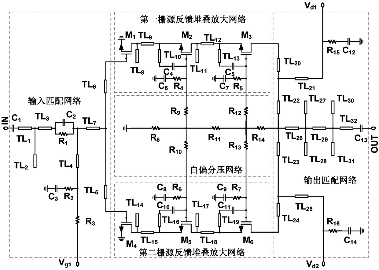
[0023] An embodiment of the present invention provides a millimeter-wave broadband high-efficiency transistor stack power amplifier, such as figure 1 As shown, it includes an input matching network, a first gate-source feedback stacked amplification network, a second gate-source feedback stacked amplification network, a self-bias voltage divider network and an output matching network; the input end of the input matching network is the input end of the entire power amplifier, Its first output end is connected to the input end of the first grid-source feedback stacking amplification network, and its second output end is co...


PUM


Abstract

The invention discloses a millimeter wave broadband high efficient transistor stacked power amplifier comprising an input match network, a first grid source feedback stacked amplification network, a second grid source feedback stacked amplification network, a self-bias potential-divider network and an output match network. According to the amplifier provided by the invention, the grid source feedback stacked amplification network is used, so that the phenomenon that the traditional transistor stacked structure amplifier is instable in millimeter waves is inhibited, and thus the grid source feedback stacked amplifier can achieve the good matching of power and efficiency; and meanwhile, the amplifier can also achieve impedance match, and has the advantages of high efficiency, high output power, high power gain and small area.

Description

technical field [0001] The invention belongs to the technical field of field effect transistor radio frequency power amplifiers and integrated circuits, and in particular relates to the design of a millimeter-wave broadband high-efficiency transistor stack power amplifier. Background technique [0002] With the rapid development of the satellite communication market that requires broadband digital transmission and high-speed satellite communication, the RF front-end transceiver is also required to develop in the direction of high integration, low power consumption, compact structure, and low price. [0003] As an important module of the transmitter, the RF and microwave power amplifier is the circuit that consumes the most energy in the entire transmitter, and its output power requirements are relatively high. When the integrated circuit process is used to design and implement the chip circuit of the RF and microwave power amplifier, its performance and cost Subject to certa...

Claims


Application Information

Patent Timeline
Patent Type & Authority Applications(China)
IPC IPC(8): H03F1/56H03F3/193H03F3/21H03F3/24H03F3/45
CPCH03F1/56H03F3/193H03F3/211H03F3/245H03F3/45179H03F2203/45156H03F2200/451
Inventor 邬海峰滑育楠陈依军胡柳林吕继平童伟王测天
Owner CHENGDU GANIDE TECH
Why Eureka
Try Eureka