Processing method of wet-method black silicon wafer and preparation method of wet-method black silicon wafer

A processing method and technology of silicon wafers, applied in the field of solar cells, can solve problems such as poor product quality, low production capacity, and low efficiency

Inactive Publication Date: 2018-11-13
ZHEJIANG JINKO SOLAR CO LTD +1
View PDF9 Cites 0 Cited by
  • Summary
  • Abstract
  • Description
  • Claims
  • Application Information

AI Technical Summary

Problems solved by technology

However, with the prolongation of the acid solution dissolution time, the concentration of metal ions in the acid solution increases gradually, which leads to a decrease in the dissolution reaction rate, and it is difficult to completely remove the metal particles, leaving metal particles on the surface of the silicon wafer, which affects the quality of the silicon wafer, making The efficiency of demetallization is greatly reduced, the time is greatly extended, and the quality of silicon wafers is affected, which in turn leads to longer time and lower efficiency of the entire silicon wafer preparation process, lower product capacity, and poor product quality

Method used


Image

  • Processing method of wet-method black silicon wafer and preparation method of wet-method black silicon wafer

Examples


preparation example Construction

[0045] The present invention also provides a method for preparing a wet-process black silicon wafer, comprising the following steps:

[0046] a) Texturing the silicon wafer with the texturing solution to obtain the texturized silicon wafer;

[0047] b) performing demetallization treatment on the textured silicon wafers to obtain demetallized silicon wafers;

[0048] The demetallization treatment is the treatment method described in the above technical scheme;

[0049] c) post-processing the demetallized silicon wafer to obtain a silicon wafer product.

[0050] Wherein, the source, type, etc. of the texturing liquid are consistent with those described in the above technical solution, and will not be repeated here. The conditions for making texture etc. are consistent with those described in the above technical solution, and will not be repeated here. The demetallization treatment in step b) is consistent with that described in the above technical solution, and will not be re...

Embodiment 1

[0057] (1) Preparation of textured silicon wafers

[0058] Place the polysilicon wafer with a clean surface in a mixed solution of hydrofluoric acid, hydrogen peroxide and silver nitrate, wherein the concentration of hydrofluoric acid is 8%, the concentration of hydrogen peroxide is 15%, and the concentration of silver nitrate is 1%; ) after soaking for 3 minutes, take it out and wash it with deionized water to obtain a textured silicon wafer.

[0059] (2) Demetallization treatment

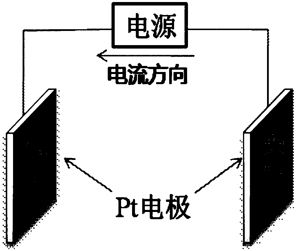
[0060] Texture silicon chip is placed in the nitric acid solution (300L) that concentration is 65%, and introduces electrochemical device, and in electrochemical device, working electrode is Pt sheet, negative electrode is Pt sheet, control voltage is 10V, under room temperature (30 °C) for an electrochemical reaction. Among them, the structure diagram of the electrochemical device is shown in figure 1 as shown, figure 1 It is the structural diagram of the electrochemical device in Example 1, ...

Embodiment 2

[0065] (1) Preparation of textured silicon wafers

[0066] The polysilicon wafer with a clean surface is placed in a mixed solution of hydrofluoric acid, hydrogen peroxide and copper nitrate, wherein the concentration of hydrofluoric acid is 10%, the concentration of hydrogen peroxide is 20%, and the concentration of copper nitrate is 2%. ) after soaking for 3 minutes, take it out and wash it with deionized water to obtain a textured silicon wafer.

[0067] (2) Demetallization treatment

[0068] Texture silicon chip is placed in the nitric acid solution (300L) that concentration is 65%, and introduces electrochemical device, and in electrochemical device, working electrode is Pt sheet, negative electrode is Pt sheet, control voltage is 10V, under room temperature (30 °C) for an electrochemical reaction. .

[0069] Blank control treatment: carried out according to the above-mentioned demetallization treatment process, the difference is that no electrochemical device is intro...


PUM


Abstract

The invention provides a processing method of a wet-method black silicon wafer and a preparation method of the wet-method black silicon wafer. The processing method provided by the invention comprisesthe following steps of introducing an electrochemical system into a demetallization cleaning liquid, and removing metal particles on the surface of a texturing silicon wafer under an electrochemicalreaction, wherein the electrochemical system takes a Pt sheet as a working electrode and takes the Pt sheet as a negative electrode. By adopting the processing method disclosed by the invention, the rate of removing the metal particles by the demetallization cleaning liquid can be greatly increased, so that the metal particles are thoroughly removed and residue is avoided, thereby highly improvingthe efficiency of the metal removal link and remarkably improving the yield of the product; in addition, the processing method can improve the utilization rate of the demetallization cleaning fluid,so that the emission of the demetallization waste liquid is greatly reduced, and the environmental pollution is reduced.

Description

technical field [0001] The invention relates to the technical field of solar cells, in particular to a method for processing a wet-process black silicon wafer and a method for preparing a wet-process black silicon wafer. Background technique [0002] At present, the energy crisis is threatening the survival and development of human beings. Compared with non-renewable petrochemical energy, solar energy resources have advantages such as cleanness and renewable energy. Therefore, a solar cell emerges as the times require, and a solar cell is a device for converting light energy into electrical energy, which can realize effective utilization of solar energy resources. Among the many types of solar cells, crystalline silicon solar cells have the highest degree of industrialization, the widest range of applications, and the most mature technology, and have always been a type of solar cell with relatively rapid development. [0003] The most critical material in crystalline silico...

Claims


Application Information

Patent Timeline
Patent Type & Authority Applications(China)
IPC IPC(8): H01L31/0236H01L31/18
CPCH01L31/02363H01L31/1804Y02P70/50
Inventor 张艳鹤金井升张昕宇金浩
Owner ZHEJIANG JINKO SOLAR CO LTD
Why Eureka
Try Eureka