

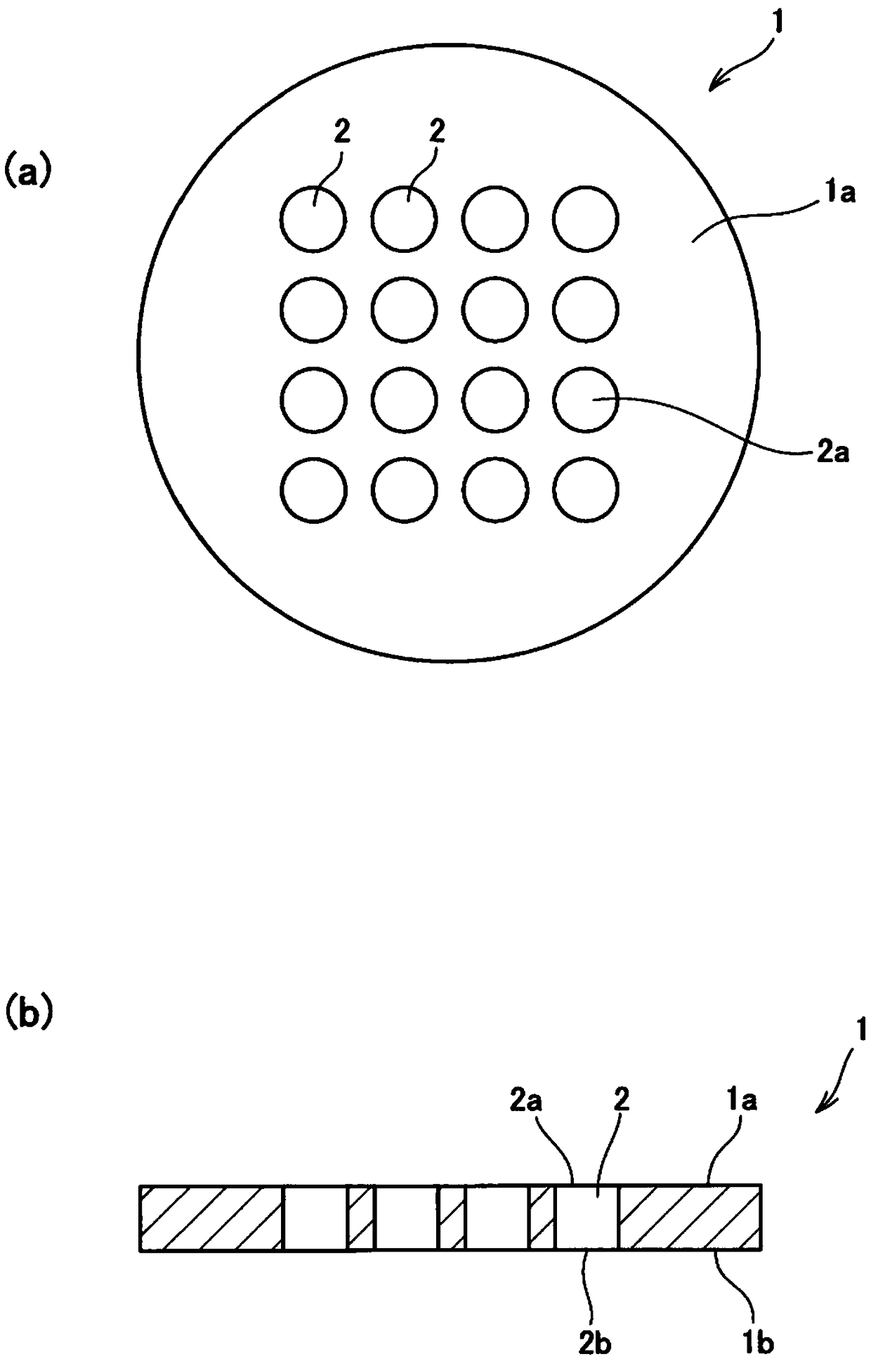
Connection substrate
一种基板、陶瓷基板的技术,应用在电气连接印刷元件、印刷元件电连接形成、印刷电路等方向,能够解决球状导电物质配置困难、陶瓷与球状导电物质热膨胀差等问题
- Summary
- Abstract
- Description
- Claims
- Application Information
AI Technical Summary
Problems solved by technology
Method used
Image

Examples
Embodiment 1
[0065] by reference Figure 1 to Figure 6 As described above, a connection board is produced.
[0066] Specifically, first, a slurry obtained by mixing the following components was prepared.
[0067] (raw material powder)
[0068]
[0069] Using the doctor blade method, the slurry is formed into a ribbon with a thickness of 300 μm after firing, and the diameter is the diameter after firing. Cut off. The obtained powder molded body was calcined (preliminarily fired) at 1240°C in the atmosphere, the substrate was placed on a molybdenum plate, and the temperature increase rate from 1300°C to 1550°C was set at 50°C in an atmosphere of hydrogen 3: nitrogen 1 °C / h, kept at 1550 °C for 2.5 hours, and fired to obtain a semi-finished substrate.
[0070] This semi-finished substrate was subjected to laser processing under the following conditions, thereby forming through-holes with the following dimensions.
[0071]
[0072]
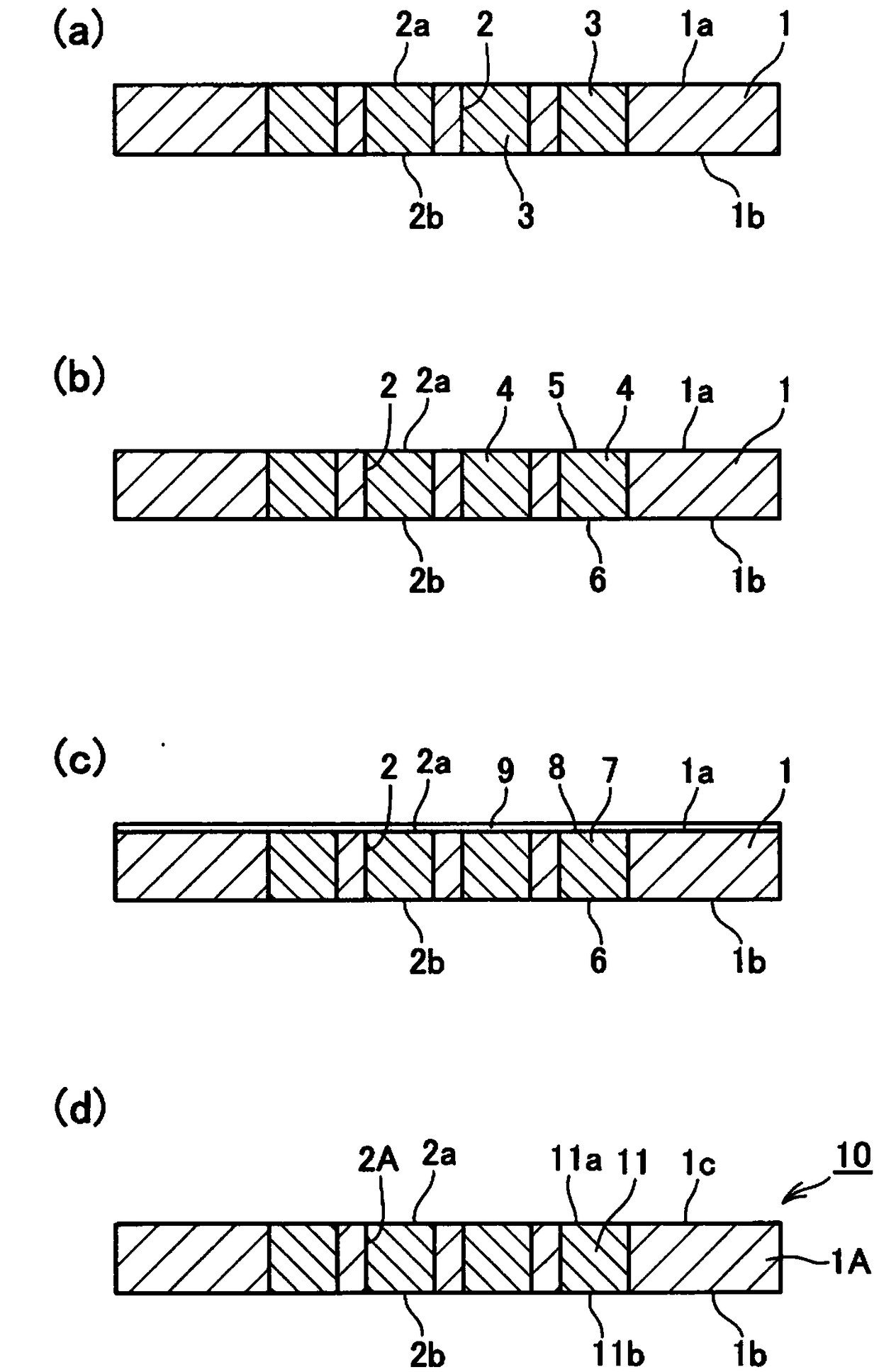
[0073] Next, the melt (dross) adhering to the...
Embodiment 2、3
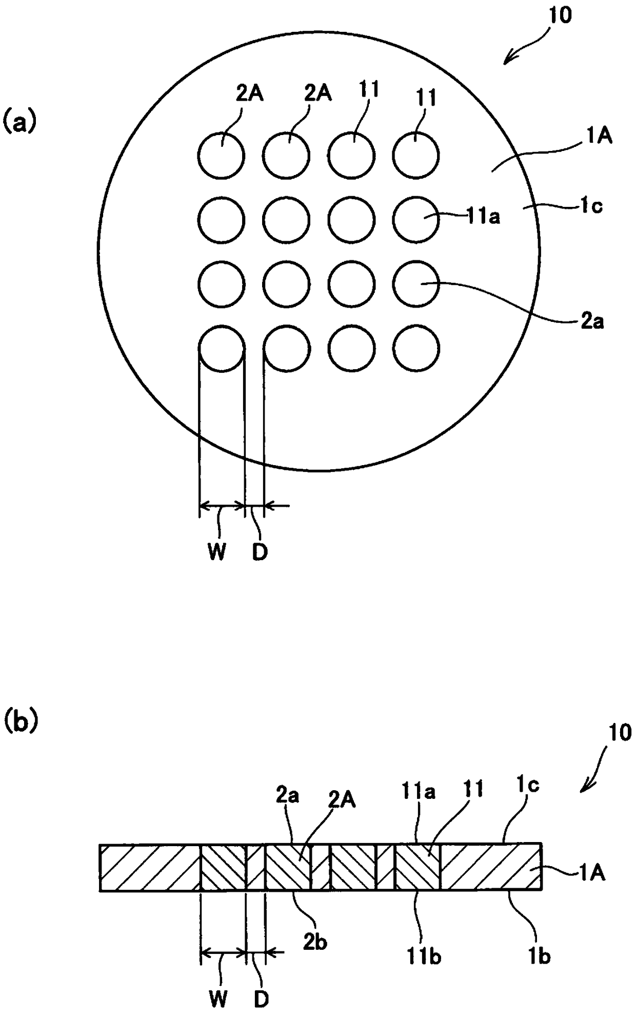
[0086] A connection substrate was produced in the same manner as in Example 1.
[0087] However, the area ratio of the pores at the cross section of the through conductor, the area ratio of the glass phase in the first part, the area ratio of the voids in the first part, the area ratio of the glass phase in the second part, and The area ratio of the voids in the second part. In order to change these parameters, adjustment was made by changing the melting temperature of the glass layer from 700°C to 750°C and 800°C to lower the viscosity of the glass.
[0088] Then, for each of the obtained ceramic substrates, the number of through-conductors in which liquid leakage was observed was measured with respect to 10,000 through-conductors provided on one ceramic substrate, and is shown in Table 1.
[0089] [Table 1]
[0090]
PUM
| Property | Measurement | Unit |
|---|---|---|
| diameter | aaaaa | aaaaa |
| diameter | aaaaa | aaaaa |
| particle diameter | aaaaa | aaaaa |
Abstract
Description
Claims
Application Information