Photoelectrochemistry type optical detector based on two-dimensional selenium nanosheet, and preparation method thereof

A photoelectrochemical and photodetector technology, used in photometry using electrical radiation detectors, nanotechnology for materials and surface science, nanotechnology, etc. Poor performance, short detection wavelength and other problems, to achieve the effect of simple and easy operation, good photoelectric detection performance, and long service life

Inactive Publication Date: 2018-12-11
SHENZHEN UNIV
View PDF6 Cites 2 Cited by
  • Summary
  • Abstract
  • Description
  • Claims
  • Application Information

AI Technical Summary

Problems solved by technology

However, this kind of photodetector has the following disadvantages: (1) the photodetector based on the wide bandgap semiconductor has a too short detection wavelength due to the large bandgap; (2) the existing two-dimensional nanomaterials have poor stability, resulting in The performance of the detector is poor; (3) The photodetector of the solid module is exposed to the air and has the disadvantage of being easily oxidized

Method used


Image

  • Photoelectrochemistry type optical detector based on two-dimensional selenium nanosheet, and preparation method thereof
  • Photoelectrochemistry type optical detector based on two-dimensional selenium nanosheet, and preparation method thereof
  • Photoelectrochemistry type optical detector based on two-dimensional selenium nanosheet, and preparation method thereof

Examples


preparation example Construction

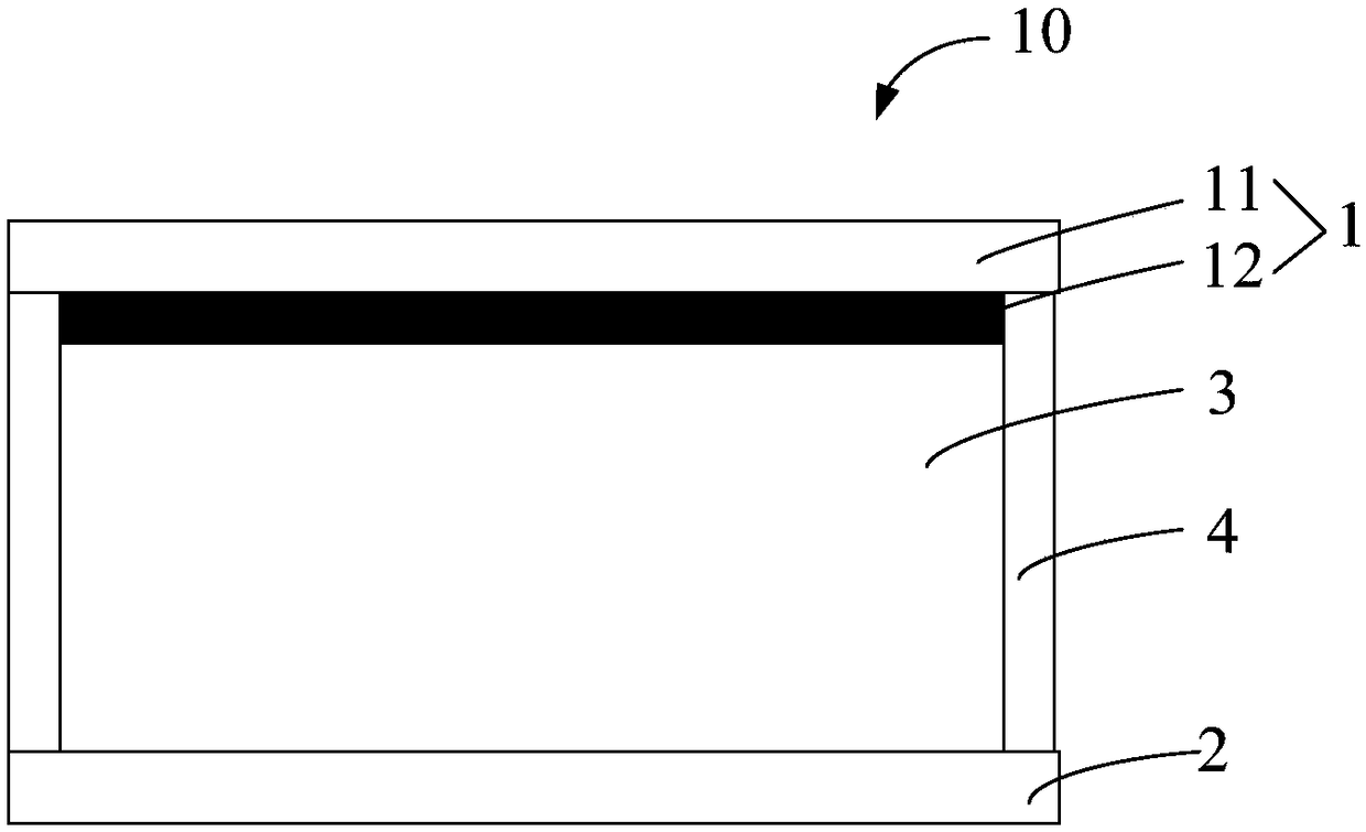
[0049] The second aspect of the present invention provides a method for preparing a photoelectrochemical photodetector based on two-dimensional selenium nanosheets, comprising the following steps:

[0050] S01, providing a selenium raw material, and stripping the selenium raw material by a liquid phase stripping method to obtain a two-dimensional selenium nanosheet;

[0051] S02, dispersing the two-dimensional selenium nanosheets in an organic solvent to form a two-dimensional selenium nanosheet dispersion, uniformly coating the two-dimensional selenium nanosheet dispersion on a conductive substrate, and drying the two-dimensional selenium nanosheet dispersion on the conductive substrate Form a semiconductor layer on it to obtain a working electrode;

[0052] S03, providing a counter electrode, assembling the working electrode and the counter electrode, so that the working electrode and the counter electrode form a sandwich structure with a cavity in the middle; then inject el...

Embodiment 1

[0077] A preparation method of two-dimensional selenium nanosheets, comprising the following steps:

[0078] (1) Add 500 mg of amorphous selenium particles into 100 ml of isopropanol. Then select the probe ultrasound 200W, ultrasound 12h. The ultrasonic on / off time was selected as 2 / 4s, and the ultrasonic was performed in an ice bath environment. After the probe is sonicated, the water bath is then used for sonication. The ultrasonic power of the water bath is 300W. Ultrasonic time is 8h. The temperature of the water bath was maintained at 10°C;

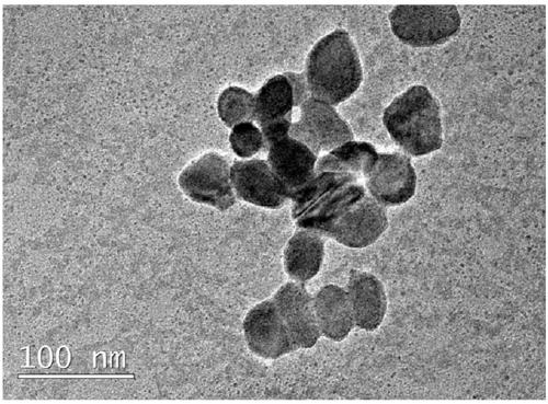
[0079] (2) Centrifuge after ultrasonication. Firstly, a centrifugal force of 2 kg is used for centrifugation for 30 minutes. Take the supernatant, and then continue to centrifuge the supernatant with a centrifugal force of 10 kg for 30 minutes to obtain a precipitate, and obtain an amorphous two-dimensional selenium nanosheet after vacuum drying.

[0080] figure 2 It is an electron microscope topography image of the two-dime...

Embodiment 2

[0083] A preparation method of two-dimensional selenium nanosheets, comprising the following steps:

[0084] (1) Add 500 mg of selenium particles with crystal structure to 100 mL of N-methylpyrrolidone. Then select the probe ultrasound 200W, ultrasound 12h. The ultrasonic on / off time was selected as 2 / 4s, and the ultrasonic was performed in an ice bath environment. After the probe is sonicated, the water bath is then used for sonication. The ultrasonic power of the water bath is 300W. Ultrasonic time is 10h. The temperature of the water bath was maintained at 15°C;

[0085] (2) Centrifuge after ultrasonication. Firstly, a centrifugal force of 1.8 kg is used, and the centrifugation is performed for 35 minutes. Take the supernatant, and then continue to centrifuge the supernatant with a centrifugal force of 10 kg for 25 minutes to obtain a precipitate, and obtain a two-dimensional selenium nanosheet with a crystal structure after vacuum drying.


PUM

PropertyMeasurementUnit
thicknessaaaaaaaaaa
sizeaaaaaaaaaa
thicknessaaaaaaaaaa

Abstract

The invention provides a photoelectrochemistry type optical detector based on a two-dimensional selenium nanosheet. The photoelectrochemistry type detector comprises a working electrode, a counter electrode and electrolyte arranged between the working electrode and the counter electrode, wherein the working electrode comprises an electric conduction substrate and a semiconductor layer arranged onone side, which faces the counter electrode, of the electric conduction substrate; the material of the semiconductor layer comprises the two-dimensional selenium nanosheet. The optical detector provided by the invention has good performance. The invention also provides a preparation method for the photoelectrochemistry type optical detector based on the two-dimensional selenium nanosheet. The preparation method comprises the following steps: providing selenium raw materials, adopting a liquid phase stripping method to strip the selenium raw materials, and obtaining the two-dimensional seleniumnanosheet; dispersing the two-dimensional selenium nanosheet in solvent to form two-dimensional selenium nanosheet dispersion liquid, evenly coating the two-dimensional selenium nanosheet dispersionliquid on the electric conduction substrate, and drying to obtain the working electrode; providing the counter electrode, injecting the electrolyte between the working electrode and the counter electrode, and packaging to obtain the optical detector. The preparation method provided by the invention is simple and easy to operate.

Description

technical field [0001] The invention relates to the field of optoelectronics, in particular to a photoelectrochemical photodetector based on two-dimensional selenium nanosheets and a preparation method thereof. Background technique [0002] Photodetectors are sensors made of materials with photoelectric effects that can realize photoelectric conversion, and their function is to realize photoelectric conversion. The mechanism is that the guided beam injected into the detector causes the stimulated transition of electrons from the valence band to the conduction band to generate photogenerated carriers (electrons and holes). And these carriers are collected by the PN junction or Schottky barrier, and finally manifested as photovoltage or photocurrent. [0003] Currently, photodetectors based on 2D nanomaterials such as black phosphorous are considered to be effective alternatives to current commercial photodetectors. However, this kind of photodetector has the following disad...

Claims


Application Information

Patent Timeline
Patent Type & Authority Applications(China)
IPC IPC(8): C01B19/02B82Y30/00B82Y40/00C03C17/22G01J1/42
CPCB82Y30/00B82Y40/00C01B19/02C01P2004/01C01P2004/04C01P2004/20C01P2004/64C03C17/22G01J1/42Y02P20/133
Inventor 张晗谢中建肖荃兰范涛健
Owner SHENZHEN UNIV
Why Eureka
Try Eureka