An enhanced high electron mobility transistor HEMT and a preparation method thereof

A high electron mobility, enhanced technology, applied in semiconductor/solid-state device manufacturing, circuits, electrical components, etc. Power device development and other issues, to achieve the effect of maintaining current characteristics, reducing static power consumption, and high current characteristics

Inactive Publication Date: 2018-12-11
PEKING UNIV SHENZHEN GRADUATE SCHOOL
View PDF4 Cites 8 Cited by
  • Summary
  • Abstract
  • Description
  • Claims
  • Application Information

AI Technical Summary

Problems solved by technology

In this process, due to the introduction of etching, the conductive channel will be severely damaged, resulting in increased d

Method used


Image

  • An enhanced high electron mobility transistor HEMT and a preparation method thereof
  • An enhanced high electron mobility transistor HEMT and a preparation method thereof
  • An enhanced high electron mobility transistor HEMT and a preparation method thereof

Examples


Embodiment 1

[0035] This embodiment takes M=4 as an example to illustrate the structure and preparation method of the enhanced HEMT, but it is not used to limit the present invention. In practical applications, M is an integer greater than or equal to 2, which can be based on the threshold voltage and current. Need to set the value of M.

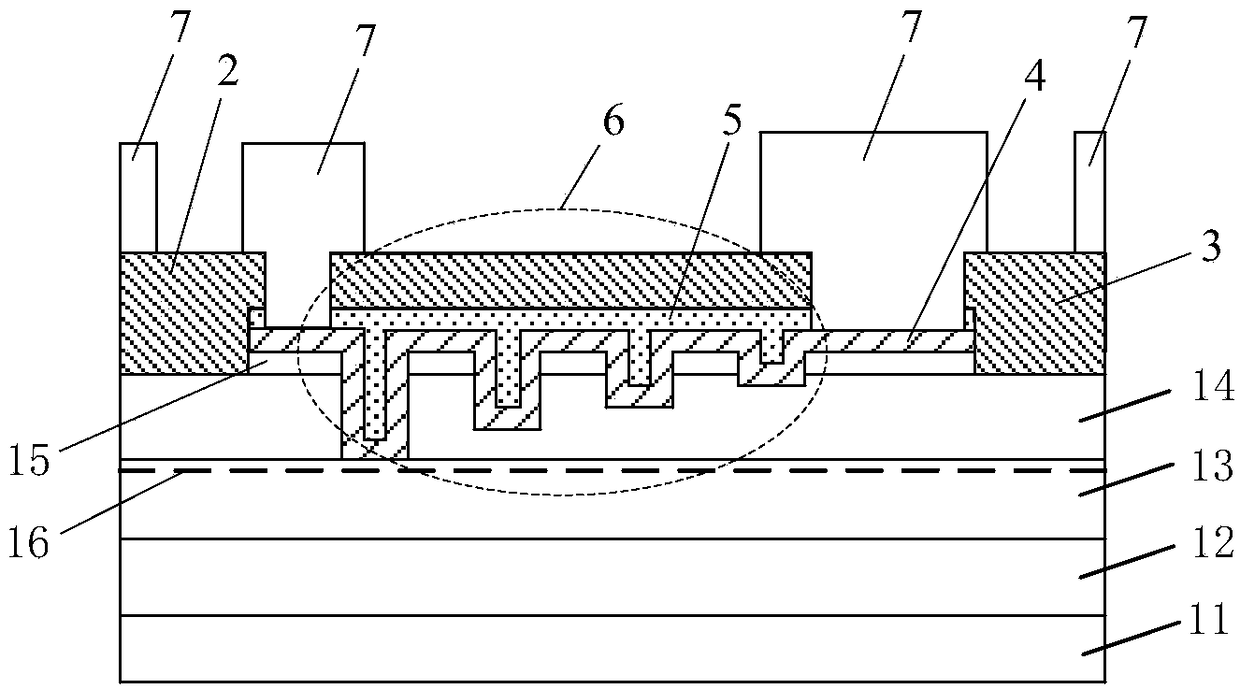
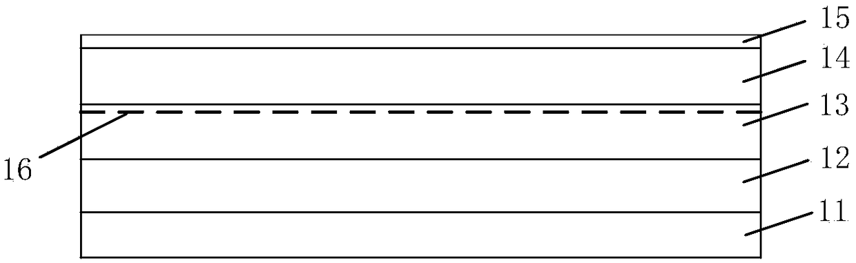
[0036] Please refer to figure 1 , figure 1 It is a schematic structural diagram of an enhanced HEMT in an embodiment of the present invention, such as figure 1 As shown, the enhanced HEMT includes a GaN epitaxial wafer, and the GaN epitaxial wafer at least includes a substrate 11 and a buffer layer 12, a channel layer 13, a barrier layer 14, and a cap layer 15 sequentially formed on the substrate 11, wherein the cap Layer 15 serves as the upper surface of the GaN epitaxial wafer, and a two-dimensional electron gas thin layer 16 is formed between the channel layer 13 and the barrier layer 14 , and the two-dimensional electron gas thin layer 16 is locate...

Embodiment 2

[0064] Different from Embodiment 1, in this embodiment, a filling dielectric layer 8 is also included between the GaN cap layer 15 and the gate dielectric layer 4. For its structure, see Figure 8 . The filling medium layer 8 can passivate and protect the surface, and is mainly used to eliminate the surface state of the material, reduce surface damage, and improve the stability and reliability of the device. In practical applications, the material filling the dielectric layer 8 can be SiO 2 、Si 3 N 4 and at least one of AlN.

[0065] based on Figure 8 In the fabrication process of the enhanced HEMT shown, the difference from Embodiment 1 is that before performing step 102, it is necessary to deposit a filling dielectric layer 8 on the upper surface of the GaN epitaxial wafer, and then perform step 102 and subsequent steps step. In practical applications, the filling dielectric layer 8 may be deposited on the upper surface of the GaN epitaxial wafer by means of LPCVD, AL...

Embodiment 3

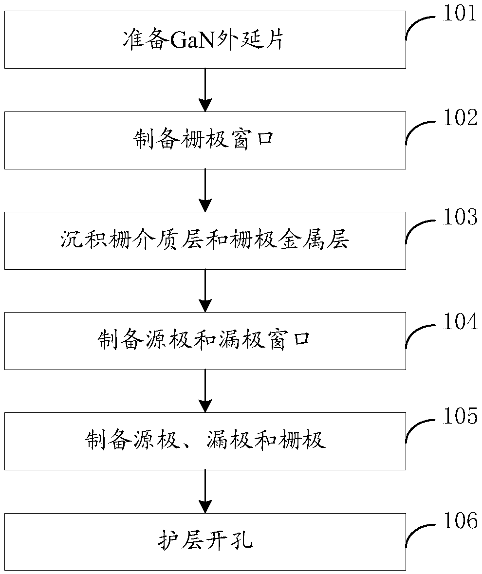
[0067] Based on the first embodiment, the difference from the first embodiment is that in this embodiment, when preparing the enhanced HEMT, the source and drain are prepared first, and the gate is prepared after the superalloy, so that the high temperature of the ohmic metal can be avoided. The influence of the alloy on the gate metal can improve the gate reliability of the device. Specifically, the flow chart of its preparation method can be found in Figure 9 , may include the following steps:

[0068] Step 201: Prepare a GaN epitaxial wafer. The specific process is the same as step 101.

[0069] Clean the GaN epitaxial wafer. After cleaning, perform the following steps:

[0070] Step 202: Prepare source and drain windows.

[0071] First realize device isolation by etching or ion implantation, and then image 3 For the GaN epitaxial wafer shown, the source region and the drain region are first defined by a photolithography process (such as the yellow light process), an...


PUM


Abstract

A enhance HEMT and a preparation method thereof, the enhanced HEMT includes a GaN epitaxial wafer, source and drain electrodes located at both ends of the GaN epitaxial wafer and a gate electrode located between the source and drain electrodes, the gate electrode comprises a plurality of concave gate grooves, wherein a gate metal layer is directly deposited on the surface of the concave gate groove to form a Schottky gate electrode, or a gate dielectric layer and a gate metal layer are sequentially deposited to form a MIS gate electrode, and the bottom of the concave gate groove is located ina barrier layer of a GaN epitaxial wafer, the total length of the concave gate groove is equal to a preset gate length, and sufficient gate control capability is ensured; The depth of each concave gate groove decreases sequentially in the direction away from the source electrode, so that the electron depletion degree in the channel decreases sequentially, and sufficient electrons are ensured in the channel, so that the characteristics of large current can be maintained on the basis of realizing the enhanced type, the on resistance of the channel is reduced, and the power consumption of the device is reduced.

Description

technical field [0001] The invention relates to the technical field of semiconductor devices, in particular to an enhanced high electron mobility transistor (High Electron Mobility Transistor, HEMT) and a preparation method thereof. Background technique [0002] With the development of efficient and complete power conversion circuits and semiconductor materials and technologies, power devices with low power consumption and high-speed characteristics have received extensive attention. Wide bandgap compound semiconductor materials and devices have become the main force in the field of semiconductor electronic devices. GaN (Gallium Nitride), represented by III-V wide bandgap compound semiconductor materials, has the characteristics of high breakdown electric field, high electron saturation drift rate and high thermal conductivity, so it is widely used in high-power, high-speed and high-voltage applications. Fabrication of power electronic devices. Among them, the enhanced HEMT...

Claims


Application Information

Patent Timeline
IPC IPC(8): H01L29/778H01L29/423H01L21/336
CPCH01L29/4236H01L29/66431H01L29/7786
Inventor 孙辉胡腾飞刘美华林信南陈东敏
Owner PEKING UNIV SHENZHEN GRADUATE SCHOOL
Why Eureka
Try Eureka