Preparation method of perovskite quantum dot array

A perovskite and quantum dot technology, applied in radiation control devices, semiconductor/solid-state device manufacturing, electrical components, etc., can solve the problem that perovskite quantum dot materials cannot meet the practical application requirements of optoelectronic devices.

Inactive Publication Date: 2018-12-11
ZHIJING NANOTECH CO LTD
View PDF5 Cites 33 Cited by
  • Summary
  • Abstract
  • Description
  • Claims
  • Application Information

AI Technical Summary

Problems solved by technology

[0003] According to one aspect of the present application, a method for preparing a perovskite quantum dot array is provided. The technical problem mainly solved by this method is that perovskite quantum dot materials cannot be patterned by photolithography like traditional quantum dot materials. As a result, perovskite quantum dot materials cannot meet the actual application requirements of optoelectronic devices

Method used


Image

  • Preparation method of perovskite quantum dot array
  • Preparation method of perovskite quantum dot array
  • Preparation method of perovskite quantum dot array

Examples


preparation example Construction

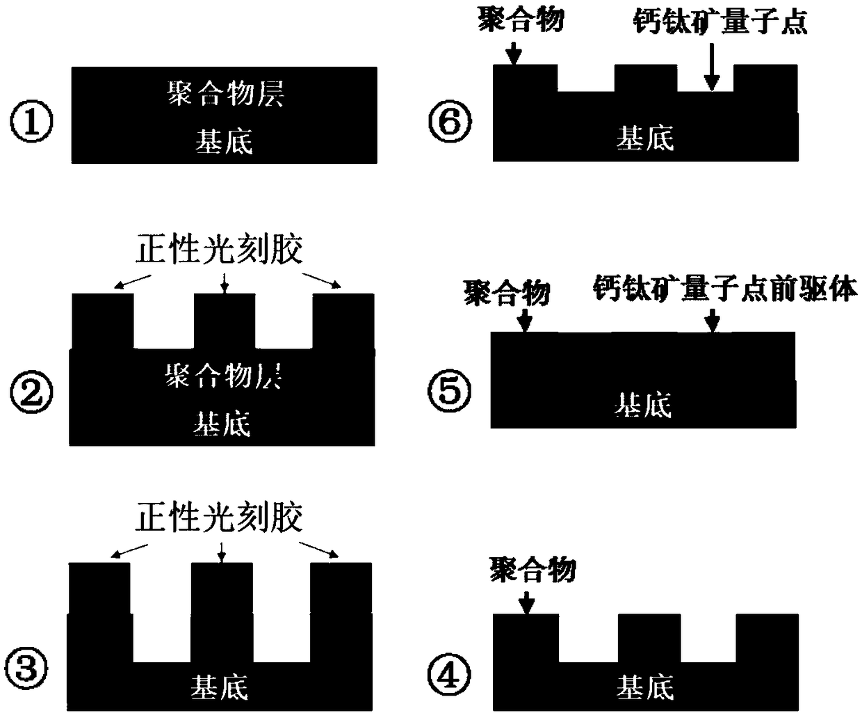
[0099] Embodiments of the present invention provide a method for preparing a perovskite quantum dot pattern, comprising:

[0100] Prepare templates required for patterning perovskite quantum dots;

[0101] transferring the perovskite quantum dot precursor solution onto the template;

[0102] Place the template attached with the perovskite quantum dot precursor solution in a dry box to complete the in-situ generation and patterning process of perovskite quantum dots;

[0103] The preparation of templates required for patterning perovskite quantum dots involves three stages: as figure 1 As shown in (1-3), the first stage is to prepare a polymer film layer on the substrate, the second stage is to use photoresist to prepare the required pattern on the polymer film layer, and the third stage is to use RIE etching After the part of the polymer layer not protected by the photoresist is removed by etching, the remaining photoresist is cleaned to obtain a polymer template with groov...

Embodiment 1

[0120] Embodiment 1 perovskite quantum dot array (pattern)

[0121] Select a 10cm*10cm Corning 0.7t glass substrate as the substrate, and drop 10wt% poly-TPD / chlorobenzene solution on the substrate. A poly-TPD layer with a wet film thickness of 3um was obtained by three-stage spin coating (200rmp 1min; 500rpm 1min; 800rpm 2min). After drying in a vacuum oven at 60°C for 30 minutes, a 1um poly-TPD polymer layer was obtained.

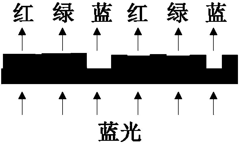
[0122] The positive photoresist is spin-coated on the surface of the polymer layer at 200rpm for 1min and 500rpm for 3min to obtain a photoresist layer with a thickness of 2.5um. Pass through the BG-401A exposure machine of Zhongdian 45 Institute to let the light pass through the mask The upper hollow part (30*100 micron pixel array) is irradiated to the corresponding area of ​​the photoresist, and is dissolved by tetramethylammonium hydroxide (TMAH) developer in the subsequent development process to form the required pattern. Use RIE-8101 reactive ion ...

Embodiment 2

[0124] Embodiment 2 perovskite quantum dot array (pattern)

[0125] A 10cm*10cm Corning 0.7t glass substrate was selected as the substrate, and the PI coating solution of DuPont RC5044 was coated on the substrate by three-stage spin coating (200rmp 1min; 500rpm 1min; 800rpm 2min) to obtain a PI layer with a wet film thickness of 2um. After drying in a vacuum oven at 120 degrees Celsius for 60 minutes, a 1.5um PI polymer layer was obtained.

[0126] The positive photoresist is spin-coated on the surface of the polymer layer at 200rpm for 1min and 500rpm for 3min to obtain a photoresist layer with a thickness of 2.5um. Pass through the BG-401A exposure machine of Zhongdian 45 Institute to let the light pass through the mask The upper hollow part (30*100 micron pixel array) is irradiated to the corresponding area of ​​the photoresist, and is dissolved by tetramethylammonium hydroxide (TMAH) developer in the subsequent development process to form the required pattern. Use RIE-810...


PUM

PropertyMeasurementUnit
thicknessaaaaaaaaaa
particle diameteraaaaaaaaaa
thicknessaaaaaaaaaa

Abstract

The invention discloses a preparation method of a perovskite quantum dot array, which is characterized in that: (1) obtaining a template; (2) filling a precursor solution of the perovskite quantum dotinto the template in the step (1), heating and drying to obtain the perovskite quantum dot array. After filling the lattice with the precursor solution, the perovskite quantum dot material in the prior art cannot be mixed with a photoresist to prepare an array pattern by photolithography by heating the perovskite quantum dot material in situ to generate the perovskite quantum dot. The perovskitequantum dot array generated in situ by the method can be applied to display devices, photodetectors and the like.

Description

technical field [0001] The application relates to a method for preparing a perovskite quantum dot array, which belongs to the technical field of quantum dot luminescent materials. Background technique [0002] Quantum dot materials refer to inorganic semiconductor nanocrystals with a particle size between 1-100nm, which have many excellent characteristics. The spectral half-wave width of quantum dot materials is relatively narrow, so the emitted light color purity is relatively high, which can significantly improve the color gamut of display devices. The emission wavelength of quantum dots can be realized by adjusting the size and composition of quantum dots, and can be controlled and adjusted in the visible spectrum according to the actual use requirements. In addition, quantum dot materials also have very high luminous efficiency, which can be realized in various Integrated applications in optoelectronic devices. At present, traditional quantum dot materials (such as CdS...

Claims


Application Information

Patent Timeline
Patent Type & Authority Applications(China)
IPC IPC(8): H01L51/56H01L51/52H01L33/50H01L27/148
CPCH01L27/14806H01L33/502H01L2933/0041H10K71/12H10K50/85
Inventor 刘瑞扩
Owner ZHIJING NANOTECH CO LTD
Why Eureka
Try Eureka