A method for the controllable preparation and patterning of two-dimensional transition metal dichalcogenide layers based on surface plasmon waves

A technology of surface plasmons, transition metals, metal selenides/tellurides, nanotechnology for materials and surface science, chemical instruments and methods, which can solve the needs of large-scale devices that are not always guaranteed, damage Degradation, time-consuming nanosheets and other issues

Active Publication Date: 2021-04-23
UNIV OF SCI & TECH OF CHINA
View PDF8 Cites 0 Cited by
  • Summary
  • Abstract
  • Description
  • Claims
  • Application Information

AI Technical Summary

Problems solved by technology

Overall, the products obtained by mechanical exfoliation and solution exfoliation showed random layer distributions, which prevented the controllable preparation of transition metal dichalcogenide nanosheets with the desired number of layers from bulk materials.
The subsequent complex screening procedures and characterization methods are not only time-consuming, but also destroy and degrade the nanosheets, making it impossible to ensure the exact number of layers
In addition, the small lateral size of transition metal dichalcogenide nanosheets prepared by the exfoliation method does not always guarantee the needs of large-scale devices.
Although the chemical vapor deposition method is a common method for preparing two-dimensional transition metal dichalcogenide materials, it is still difficult to control the number of layers of the transition metal dichalcogenide material and the polycrystalline layer caused by the grain boundary.
[0004] Therefore, the controllable preparation of 2D transition metal dichalcogenide materials with tunable layers and large area remains a great challenge.

Method used


Image

  • A method for the controllable preparation and patterning of two-dimensional transition metal dichalcogenide layers based on surface plasmon waves
  • A method for the controllable preparation and patterning of two-dimensional transition metal dichalcogenide layers based on surface plasmon waves
  • A method for the controllable preparation and patterning of two-dimensional transition metal dichalcogenide layers based on surface plasmon waves

Examples


preparation example Construction

[0029] The present invention provides a method for the controllable preparation and patterning of layers of two-dimensional transition metal dichalcogenides based on surface plasmon waves, comprising the following steps:

[0030] A laser with a wavelength of 670nm is used to irradiate the surface of a transition metal disulfide sample placed in an aqueous solution at the maximum incident angle of total internal reflection;

[0031] Controlling the output power of the laser for exciting surface plasmon waves to obtain a transition metal dichalcogenide with a controllable number of layers; the number of layers is 1, 2 or 3 layers;

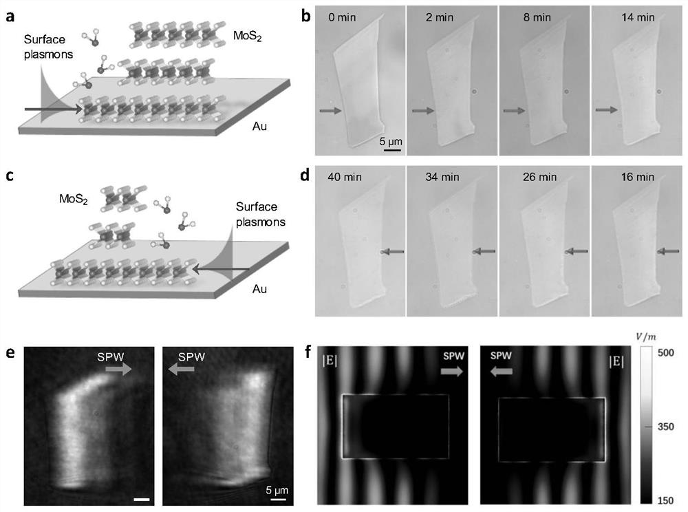
[0032] The propagation direction and etching time of the surface plasmon wave are adjusted to obtain patterned layered transition metal dichalcogenides.

[0033] The invention adopts the laser with the wavelength of 670nm to irradiate the surface of the transition metal disulfide sample placed in the aqueous solution at the maximum incident angle of ...

Embodiment 1

[0044] Example 1: Exciting Surface Plasmon Waves

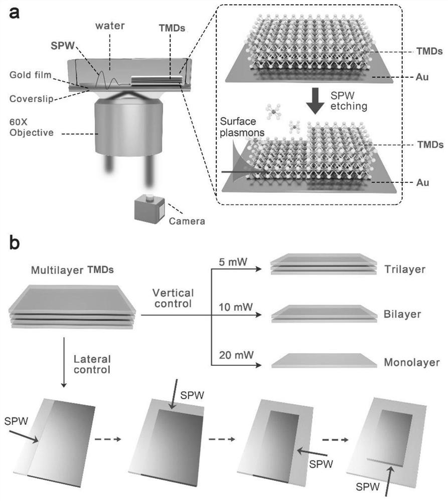
[0045] Layer-number-controllable fabrication and patterning of 2D transition metal dichalcogenides is achieved in surface plasmon resonance microscopy, see figure 1 . On the basis of an inverted total internal reflection fluorescence microscope (Nikon Ti-E), a high numerical aperture oil immersion objective lens (60X, NA=1.49) was selected to construct a surface plasmon resonance microscope. Gold-plated chips were prepared by evaporating 2nm chrome as an adhesion layer on a BK-7 glass cover slip, and then evaporating 47nm gold layer. A laser diode (coherent OBIS, wavelength = 670nm, output power adjustable from 0.5 to 70mW) was used as the light source, and a polarizer was inserted in the optical path to generate p-polarized light to excite surface plasmon waves. The system includes a laser light source, a collimator, a polarizer, a condenser, a scanning galvanometer, a lens, an oil immersion objective, a gold-plated chip, a...

Embodiment 2

[0047] Example 2: Controllable preparation of molybdenum disulfide with adjustable layers

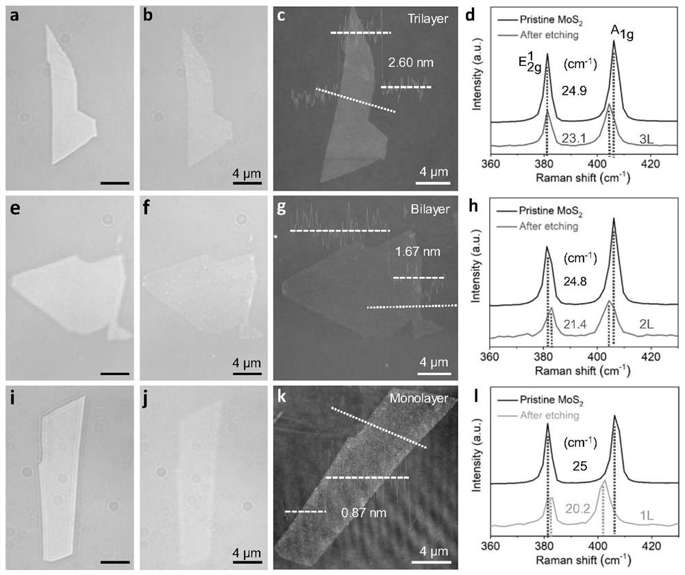
[0048] The etching rate of molybdenum disulfide nanosheets depends on the output power of the laser that excites surface plasmon waves, and the layer number control of molybdenum disulfide (such as single layer, double layer and triple layer) can be realized by directly adjusting the output power of the laser. figure 2 In a, e and i are the optical images of the molybdenum disulfide nanosheets that were initially exfoliated. When the output power of the laser is 5mW, 10mW and 20mW, the optical images of the molybdenum disulfide nanosheets after etching are recorded to obtain three-layer, double-layer layer and monolayer of molybdenum disulfide. figure 2 In b, f and j are the optical images of three-layer, two-layer and single-layer MoS2, respectively. The image and the corresponding height map of the atomic force microscopy experiment show that the thickness of the molybdenum disulfi...


PUM

PropertyMeasurementUnit
wavelengthaaaaaaaaaa
thicknessaaaaaaaaaa
thicknessaaaaaaaaaa

Abstract

The present invention provides a method for the controllable preparation and patterning of two-dimensional transition metal dichalcogenide layers based on surface plasmon waves, comprising the following steps: using a laser with a wavelength of 670 nm to irradiate the The surface of the sample placed in an aqueous solution; the output power of the laser that excites the surface plasmon wave is adjusted to obtain a transition metal disulfide with a controllable number of layers; the number of layers is 1 layer, 2 layers or 3 layers; the surface plasmon wave is adjusted The propagation direction and etching time of the patterned layered transition metal dichalcogenides are obtained. Taking molybdenum disulfide as a representative example, the layer number control of molybdenum disulfide is realized by adjusting the output power of the light source that excites surface plasmon waves. The simultaneous etching process depends on the propagating direction of the surface plasmon waves, enabling the patterning of various MoS2 homostructures. The invention is easy to operate, has very little pollution and damage to the sample, and the surface of the sample after treatment is complete and clean.

Description

technical field [0001] The invention belongs to the technical field of preparation of two-dimensional nanomaterials, and in particular relates to a preparation method for the controllable preparation and patterning of two-dimensional transition metal dichalcogenide layers based on surface plasma waves. Background technique [0002] Two-dimensional transition metal dichalcogenide materials have become a hotspot in basic scientific research due to their wonderful layer-dependent properties, especially in the fields of optoelectronics, spintronics, and recently, valleytronics. The reduction of the number of layers of 2D transition metal dichalcogenides to the atomic layer induces significant changes in the electronic structure and crystal symmetry, which in turn affects their optical, electrical, and magnetic properties. For example, due to the bandgap change and interband optical selection from bulk to monolayer, in monolayer MX 2 Strong photoluminescence and valley polarizat...

Claims


Application Information

Patent Timeline
Patent Type & Authority Patents(China)
IPC IPC(8): C01G39/06C01G41/00C01B19/00C01B19/04B82Y30/00B82Y40/00
CPCB82Y30/00B82Y40/00C01B19/002C01B19/007C01G39/06C01G41/00C01P2004/20
Inventor 刘贤伟周晓丽
Owner UNIV OF SCI & TECH OF CHINA
Why Eureka
Try Eureka