A kind of cadmium telluride solar cell and preparation method thereof
A solar cell, cadmium telluride technology, applied in circuits, electrical components, photovoltaic power generation and other directions, can solve the problems of low conversion efficiency of solar cells, battery attenuation, complicated preparation process of back contact materials, etc., to improve the collection and transfer capacity. , The effect of reducing the interface loss and excellent long-term stability
- Summary
- Abstract
- Description
- Claims
- Application Information
AI Technical Summary
Problems solved by technology
Method used
Image
Examples
preparation example Construction
[0036] The present invention also provides a preparation method of a cadmium telluride solar cell, characterized in that the preparation method comprises the following steps:
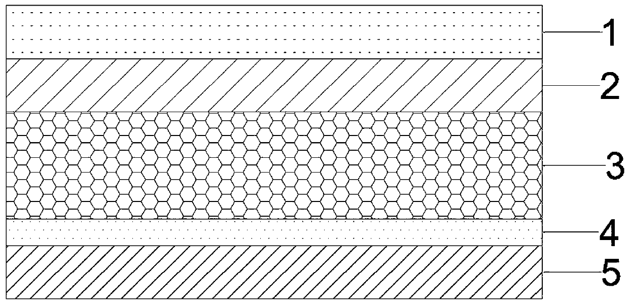
[0037] (1) providing a substrate layer, depositing cadmium sulfide on the substrate layer to obtain a window layer;
[0038] (2) Depositing cadmium telluride on the window layer to obtain a light absorbing layer;
[0039] (3) Magnetron sputtering copper-doped molybdenum oxide on the light absorbing layer to obtain a back contact layer;
[0040] (4) Etching the back contact layer with an acid solution to form a back contact layer with a textured structure;
[0041] (5) depositing a back electrode layer on the back contact layer;
[0042] (6) Annealing treatment.
[0043] Preferably, the material of the back electrode layer is metal molybdenum or metal nickel.
[0044] Preferably, the deposition method in step (4) is magnetron sputtering.
[0045] Preferably, the thickness of the back contact layer i...
Embodiment
[0056] Effect of the thickness of textured back electrode on the performance of CdTe thin film battery
[0057] 1. Experimental samples: cadmium telluride thin-film battery sample 1, sample 2, sample 3, sample 4, and sample 5. The preparation methods and parameters of the five samples are the same except for the thickness of the back contact layer;
[0058] 2. Experimental method: use the method described in GB / T 6495.1-1996 for performance testing;
[0059] 3. Experimental results: See Table 2.
[0060] Table 3 The influence of back contact layer thickness on the performance of cadmium telluride thin film battery
[0061]
[0062]
[0063] It can be seen from Table 3 that when the thickness of the back contact layer is 20nm, the charge and discharge efficiency, open circuit voltage, short circuit current and fill factor of the battery all reach the maximum value, and the photoelectric conversion efficiency of the battery is the highest at this time.
[0064] Example
...
PUM
| Property | Measurement | Unit |
|---|---|---|
| thickness | aaaaa | aaaaa |
| thickness | aaaaa | aaaaa |
| thickness | aaaaa | aaaaa |
Abstract
Description
Claims
Application Information


