A vertical cavity surface emitting silicon substrate GaN laser based on a dielectric Bragg mirror and a preparation method thereof

A technology of Bragg reflector and vertical cavity surface emission, which is applied in the direction of lasers, laser components, semiconductor lasers, etc., can solve the problems of complex process, time-consuming and difficult to obtain high quality of semiconductor Bragg reflectors, and achieve the benefit of large-scale The effect of mass production, excellent thermal and electrical conductivity, and easy substrate

Inactive Publication Date: 2019-01-04
NANJING INST OF TECH
View PDF2 Cites 18 Cited by
  • Summary
  • Abstract
  • Description
  • Claims
  • Application Information

AI Technical Summary

Problems solved by technology

[0004] The technical problem to be solved by the present invention is to provide a vertical cavity surface emitting silicon substrate GaN laser based on a dielectric Bragg reflector and its preparation method, which can solve the semiconductor Bragg problem that the existing GaN vertical cavity surface emitting laser i...

Method used


Image

  • A vertical cavity surface emitting silicon substrate GaN laser based on a dielectric Bragg mirror and a preparation method thereof
  • A vertical cavity surface emitting silicon substrate GaN laser based on a dielectric Bragg mirror and a preparation method thereof
  • A vertical cavity surface emitting silicon substrate GaN laser based on a dielectric Bragg mirror and a preparation method thereof

Examples


Embodiment Construction

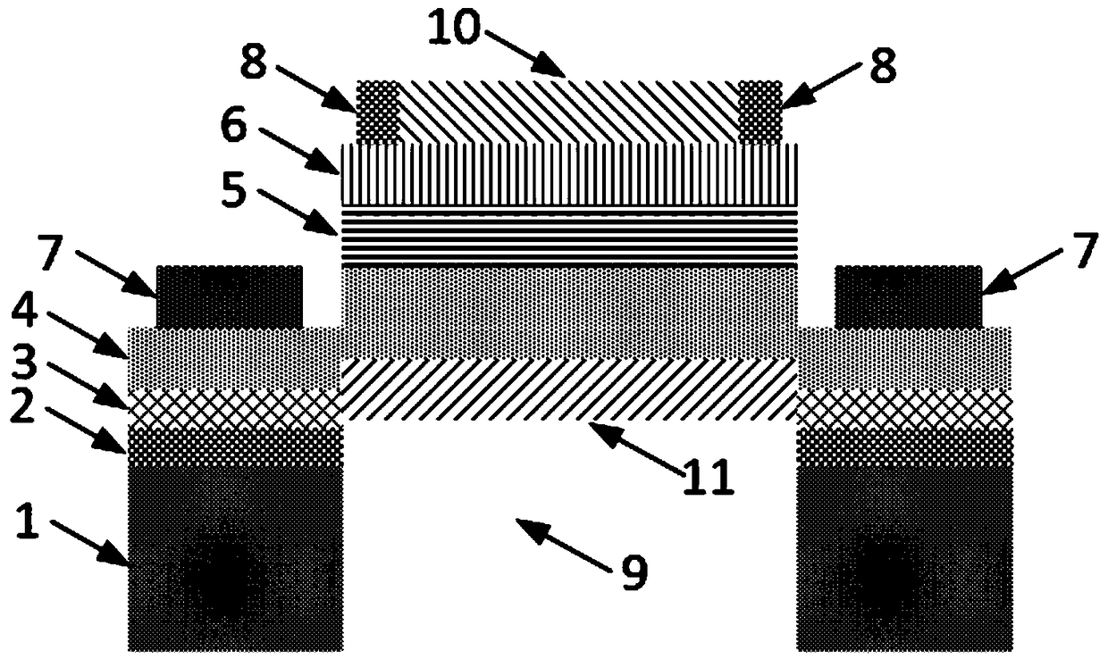
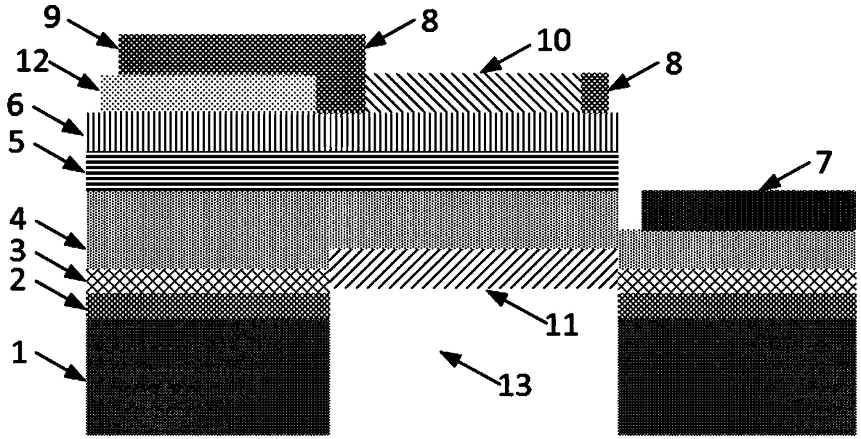
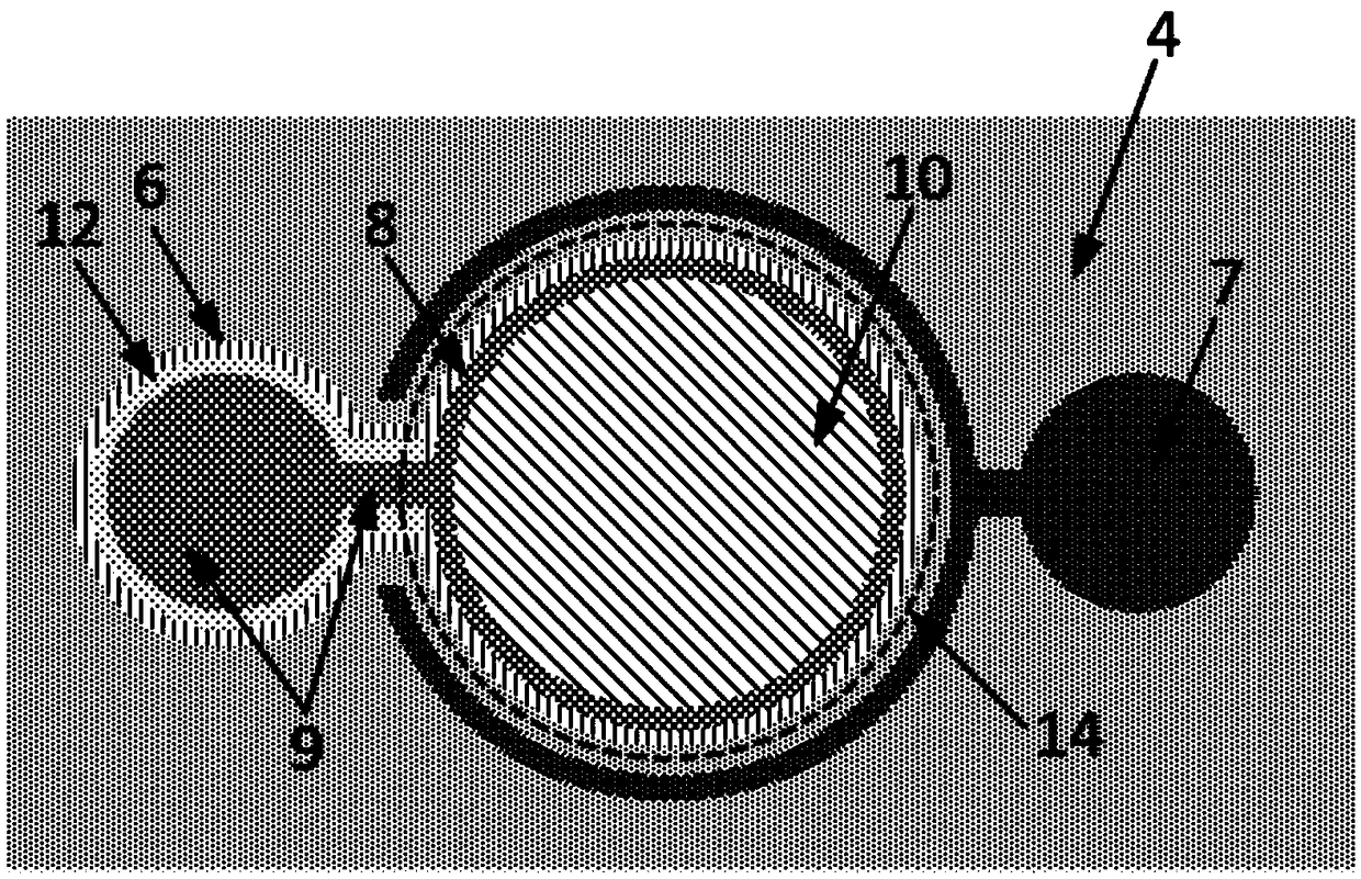
[0038] Such as figure 1 , figure 2 with image 3 As shown, a vertical cavity surface emitting silicon substrate GaN laser based on a dielectric Bragg mirror uses a silicon substrate nitride wafer as a carrier, including a silicon substrate layer 1, an AlN layer 2 disposed on the silicon substrate layer 1, An AlGaN layer 3 disposed on the AlN layer 2 , a vertical resonant microcavity 14 disposed on the AlGaN layer 3 , an insulating isolation layer 12 , an n-type electrode 7 and a p-type electrode.

[0039] The vertical resonant microcavity 14 is composed of an n-GaN layer 4, an InGaN multi-quantum well layer 5 disposed on the n-GaN layer 4, a p-GaN layer 6 disposed on the InGaN multi-quantum well layer 5, and a p-GaN multi-quantum well layer disposed on the p-GaN layer 6 and a bottom mirror 11 disposed on the lower surface of the n-GaN layer 4. The p-type electrode is composed of the connected p-type electrode conductive region 8 and p-type electrode bonding region 9 . The...


PUM

PropertyMeasurementUnit
Thicknessaaaaaaaaaa

Abstract

The invention discloses a vertical cavity surface emitting silicon substrate GaN laser based on a dielectric Bragg mirror and a preparation method thereof, Using deep silicon etching technology, the silicon substrate on the bottom of the device is stripped completely, and then the AlN layer, AlGaN layer and part of n-GaN layer are etched off from the back by inductively coupled plasma reactive ionetching technology. GaN lay to regulate that length of the vertical resonant microcavity; The mirrors at the top and bottom of the vertical resonant microcavity are realized by electron beam evaporation technology to deposit dielectric Bragg mirrors. The insulating insulation layer and the top mirror located below the p-type electrode bonding region are simultaneously accomplished using a one-step electron beam evaporation process. During the fabrication process, tunable wavelength and controllable laser direction can be obtained by adjusting the related parameters to achieve the laser wavelength and emission direction selection, so as to obtain an electrically pumped GaN laser. The vertical cavity surface emitting silicon substrate GaN laser based on the dielectric Bragg mirror has low cost, simple preparation process and can be used in a plurality of fields.

Description

technical field [0001] The invention relates to the field of information materials and devices, in particular to a vertical cavity surface emitting silicon substrate GaN laser based on a dielectric Bragg reflector and a preparation method thereof. Background technique [0002] Vertical cavity surface emitting laser (VCSEL) is a new type of semiconductor laser with great development prospects, and it is a major breakthrough in the integration of photonic devices. The vertical cavity surface emitting laser is different from the conventional end surface emitting laser. The end surface emitting laser emits light sideways, while the output light of the vertical cavity surface emitting laser is perpendicular to the surface of the resonant cavity. This difference in the orientation of the optical cavity makes the performance of the vertical cavity surface emitting laser much better than that of the conventional end surface emitting laser. The vertical emission of the laser makes i...

Claims


Application Information

Patent Timeline
IPC IPC(8): H01S5/183H01S5/187H01S5/343
CPCH01S5/18361H01S5/187H01S5/34333
Inventor 蔡玮王永进
Owner NANJING INST OF TECH
Why Eureka
Try Eureka