A manufacturing process of a vertical silicon nanowire transistor

A technology of silicon nanowires and manufacturing processes, which is applied in semiconductor/solid-state device manufacturing, semiconductor devices, electrical components, etc., can solve problems such as device structure and characteristic asymmetry, and achieve the effect of symmetrical structure and performance.

Inactive Publication Date: 2019-01-11
SHANGHAI HUALI MICROELECTRONICS CORP
View PDF3 Cites 2 Cited by
  • Summary
  • Abstract
  • Description
  • Claims
  • Application Information

AI Technical Summary

Problems solved by technology

[0009] The invention improves the manufacturing process of the original vertical silicon nanowire transistor, and specifically solves the problem of device structure and characteristic asymmetry caused by the surrounding gate blocking part of the source-side ion implantation.

Method used


Image

  • A manufacturing process of a vertical silicon nanowire transistor
  • A manufacturing process of a vertical silicon nanowire transistor
  • A manufacturing process of a vertical silicon nanowire transistor

Examples


Embodiment 2

[0049] Embodiment 2 is used to manufacture flash storage unit devices, and the dose of ion implantation required for the process flow is at 10 16 / cm 2 the following:

[0050] The only difference from Example 1 is that the gate dielectric SiO in Example 1 2 Replaced with the ONO layer used for charge storage in flash memory cells. In step c and step d of embodiment 1, the process step of silicon pillar thermal oxidation is omitted, and the first dielectric layer (SiO 2 ) after the formation of chemical vapor deposition ONO layer (SiO 2 -Si 3 N 4 -SiO 2 ) gate dielectric 710 and polysilicon gate 810, such as Figure 12 and Figure 13 shown. The top polysilicon and top ONO layer are then etched away. The rest of the process flow is the same as that of Embodiment 1, so that the flash memory with the vertical silicon nanowire transistor as the storage unit can be manufactured.

Embodiment 1

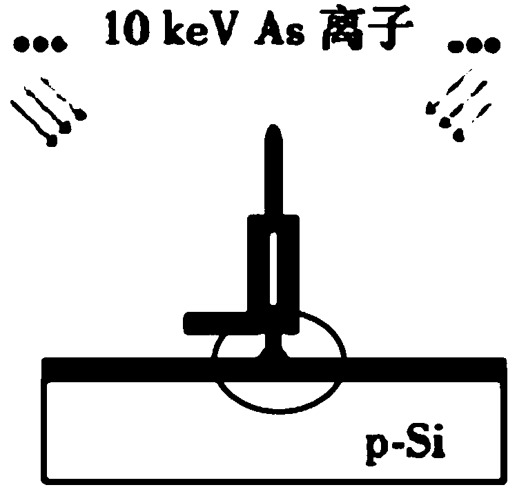
[0051] The dose of ion implantation required for the process flow of embodiment 1 and embodiment 2 is at 10 16 / cm 2 Below, if the dose of ion implantation exceeds 10 16 / cm 2 , silicon, polysilicon, SiO 2 If the structure of the dielectric layer is destroyed by the implanted ions, the cases of Embodiment 3 and Embodiment 4 apply, and ion implantation will not be used as a doping method.

Embodiment 3

[0052] Embodiment 3 is used to manufacture logic MOSFET devices, and the dose of ion implantation required for the process flow is at 10 16 / cm 2 above:

[0053] At this time, due to the large dose of ion implantation, silicon, polysilicon, SiO 2 The structure of the dielectric layer is damaged, so ion implantation is not used as a doping method, and in-situ doping technology will be used for impurity doping during chemical vapor deposition. In-situ doping reduces an ion implantation process and can achieve uniform doping.

[0054] Specifically, in the first step of the process in step a, instead of using ion implantation for doping, a dopant gas, such as AsH 3 ,PH 3 , B 2 h 6 When the gas is fed into the reaction chamber, the doping of arsenic, phosphorus, boron and other impurities in the epitaxy can be realized. In this embodiment, PH is introduced into the vapor phase epitaxy reaction chamber of silicon 3 and SiH 4 , the doping of phosphorus is carried out by the ...


PUM

PropertyMeasurementUnit
thicknessaaaaaaaaaa
thicknessaaaaaaaaaa
thicknessaaaaaaaaaa

Abstract

The invention provides a manufacturing process of a vertical silicon nanowire transistor. By improving the fabrication technology of vertical silicon nanowire transistor, the invention avoids the blocking effect of the enclosure gate of the vertical silicon nanowire transistor when ion implanting the source and the drain in the prior art, and the blocking effect can cause the asymmetry of the device performance caused by the non-uniform doping of the source and the drain, thus causing the circuit design and the device reliability to encounter problems. The invention adopts a new process step,solves the problem of device structure and characteristic asymmetry caused by blocking part of source end ion implantation by the vertical silicon nanowire transistor enclosure gate, enables the vertical silicon nanowire transistor structure and performance to be symmetrical, does not depend on the selection of source and drain, and thus the circuit design will greatly benefit.

Description

technical field [0001] The invention relates to the field of semiconductor integrated circuit manufacturing, and in particular to a manufacturing process method for a vertical silicon nanowire transistor. Background technique [0002] In order to improve the integration level of integrated circuits and the performance of chips, with the development of integrated circuit MOS device technology, the critical dimensions of devices are getting smaller and smaller. For the traditional single-gate planar process, the gate length of the device cannot be reduced indefinitely, and a series of secondary effects appear as the device size shrinks, collectively referred to as the short channel effect. Conventional electrical characteristics in the case of long-channel devices tend to become poor in the case of short-channel devices. In order to overcome the impact of the short channel effect on the performance and reliability of small-sized MOS devices, some new device structures have em...

Claims


Application Information

Patent Timeline
Patent Type & Authority Applications(China)
IPC IPC(8): H01L21/336
CPCH01L29/66477
Inventor 顾经纶
Owner SHANGHAI HUALI MICROELECTRONICS CORP
Why Eureka
Try Eureka