Near-infrared response photodetector of microlens trap structure and preparation method thereof

A technology of photodetector and light trapping structure, which is applied in the field of photodetector to achieve the effect of improving comprehensive performance

Inactive Publication Date: 2019-01-11
THE 44TH INST OF CHINA ELECTRONICS TECH GROUP CORP
View PDF6 Cites 7 Cited by
  • Summary
  • Abstract
  • Description
  • Claims
  • Application Information

AI Technical Summary

Problems solved by technology

[0006] In view of this, in order to solve the problem of conflicting responsivity and temperature coefficient of breakdown voltage, responsivity and response time of traditional APD devices, the present invention proposes a near-infrared responsive photodetector with microlens trapping structure

Method used


Image

  • Near-infrared response photodetector of microlens trap structure and preparation method thereof
  • Near-infrared response photodetector of microlens trap structure and preparation method thereof
  • Near-infrared response photodetector of microlens trap structure and preparation method thereof

Examples


Embodiment Construction

[0039] A near-infrared responsive photodetector with a microlens light-trapping structure of the present invention will be further described below in conjunction with the accompanying drawings.

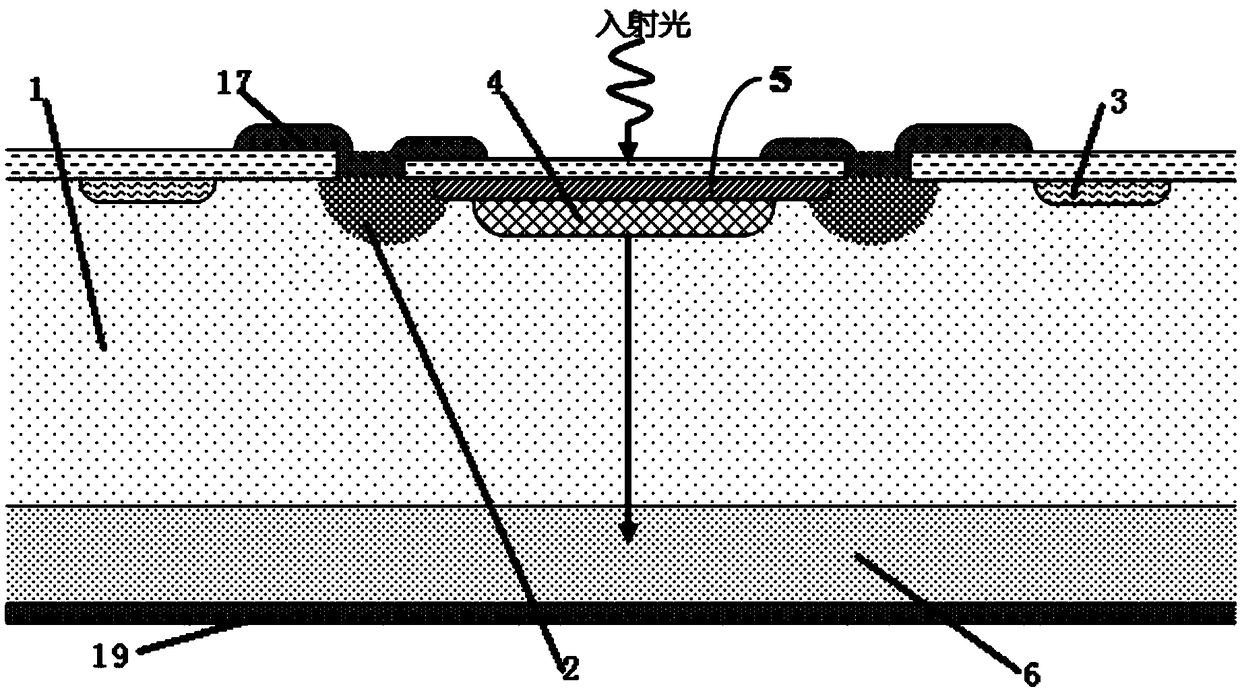
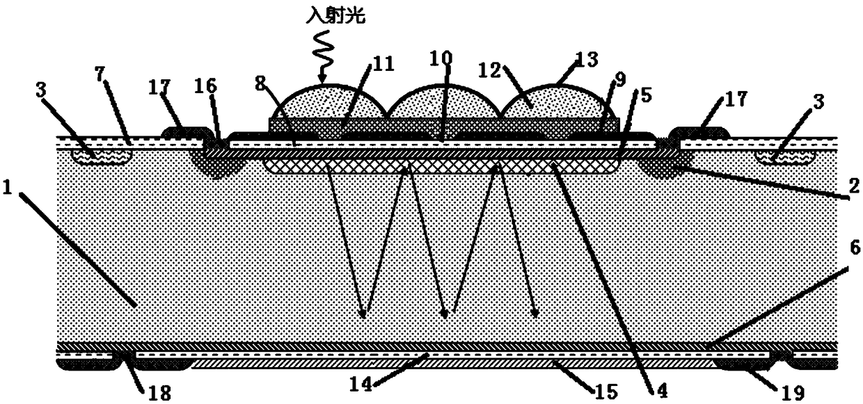
[0040] figure 1 It is a schematic diagram of the structure of a traditional pull-through silicon APD device; figure 2 It is a schematic diagram of the structure of a near-infrared response enhanced silicon APD device with a microlens light trapping structure, such as figure 1 , figure 2 As shown, the intermediate structure (i.e. absorbing layer, avalanche multiplication layer, highly doped charge layer, guard ring, cut-off ring, Passivation layer and cathode electrode) are exactly the same as the middle structure of the existing detector (the thickness of the absorbing layer is different), and the function played by the middle structure is also exactly the same as the prior art. The difference between the present invention and the prior art is that , The detector of the present i...


PUM


Abstract

The invention belongs to the technical field of photoelectric detectors and relates to a near-infrared response photoelectric detector with a microlens trap structure and a preparation method thereof.A photosensitive region passivation layer is arranged in the central region of the upper surface of the absorption layer, and a front mirror, a microlens cushion layer and a microlens array are arranged on the upper surface of the photosensitive passivation layer from bottom to top in sequence. The thickness of the microlens cushion layer is the focal length of the microlens, and the front mirroris provided with a plurality of small light through holes. The invention has the advantages that: from the principle of near infrared response enhancement of microlens trap structure, it can be seenthat the response enhancement is realized by increasing the absorption length of light in the absorption layer through the reflection of the mirror, which does not depend on the increase of the thickness of the absorption layer, so the breakdown voltage temperature coefficient and the response time of the detector will not be increased. Moreover, the temperature coefficient of breakdown voltage and the response speed of the device can be reduced by further reducing the thickness of the absorption layer, so that the comprehensive performance of the near-infrared silicon APD photodetector can begreatly improved.

Description

technical field [0001] The invention belongs to the technical field of photodetectors, and in particular relates to a near-infrared responsive photodetector with a microlens light-trapping structure and a preparation method thereof. Background technique [0002] Near-infrared (780nm~1100nm) silicon APD photodetectors have the advantages of high sensitivity, large gain, small dark current, and low cost. They are widely used in laser ranging, low-light detection, precision guidance, and optical alignment. . [0003] Near-infrared silicon APD photodetectors generally adopt a reach through N+-p-π-P+ device structure. Compared with ordinary PN or PIN APDs, they have the advantage of relatively small breakdown voltage. APD employs the most device configurations. It is mainly composed of a highly doped charge layer (N+), an avalanche multiplication region (p), an intrinsic absorption layer (π), an anode contact layer (P+), a guard ring, a stop ring, an anti-reflection film and an...

Claims


Application Information

Patent Timeline
Patent Type & Authority Applications(China)
IPC IPC(8): H01L31/107H01L31/0232H01L31/18
CPCH01L31/02327H01L31/107H01L31/1804
Inventor 黄建李睿智江海波高建威郭培黄烈云
Owner THE 44TH INST OF CHINA ELECTRONICS TECH GROUP CORP
Why Eureka
Try Eureka