Method for preparing skin of robot with high flexibility
A robotic and high-strength technology, applied in instruments, manipulators, manufacturing tools, etc., can solve problems such as limiting the application range of electronic skin, hindering chip performance, and ineffective combination of electronic chips and matrix materials, and achieves benefits such as chip performance, enhanced elasticity, The effect of expanding the scope of application
- Summary
- Abstract
- Description
- Claims
- Application Information
AI Technical Summary
Problems solved by technology
Method used
Image
Examples
Embodiment 1
[0020] 1: Use plasma equipment to etch 0.1-60% of styrene-type TPE, olefin-type TPE, diene-type TPE, vinyl chloride-type TPE or polyurethane-type TPE matrix materials at a pressure of 0.1-100 MPa and a power of 600-2000 watts. Minutes, a flexible elastic matrix is prepared. The repeating unit of the flexible elastic matrix is 1-100 microns, and the pitch is 1-100 microns. Dot matrix, strip matrix or strip grating, and then micro The nanofabrication process introduces 1-100nm particles on the surface of the repeating unit, and further performs micro-nano patterning design on the surface of the pre-fabricated flexible substrate.
[0021] Two: Spray 0.001-100 mg / mL graphene or carbon nanotube solution on the surface of the patterned substrate as a conductive layer, and control the thickness of the liquid layer to 30-150 microns.
[0022] Three: Coating a layer of silane coupling agent, titanate coupling agent or zirconium coupling agent on the sensor electronic chip component...
Embodiment 2
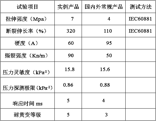
[0024] Through the lattice design program, first use plasma equipment to treat vinyl chloride TPE at 1000W power and 10MPa pressure for 20 minutes to prepare a lattice surface patterned TPE matrix with a repeating unit size of 10 microns and a spacing of 10 microns, and then use photolithography The surface is further micro-nano-processed by the etching method to obtain a micro-nano patterned matrix with uniform distribution of 50 nm particles on the matrix points. Apply 10 mg / mL graphene solution on the surface of the patterned substrate, and control the thickness of the liquid layer to be 50 microns. The pressure-sensitive flexible electronic skin can be prepared by treating the pressure sensor electronic chip with a titanate coupling agent, and then implanting it into the TPE matrix by embedding.
PUM
| Property | Measurement | Unit |
|---|---|---|
| Concentration | aaaaa | aaaaa |
| Thickness | aaaaa | aaaaa |
Abstract
Description
Claims
Application Information
