Composition for forming organic film, substrate for manufacturing semiconductor apparatus, method for forming organic film, patterning process, and polymer
A technology of organic film and composition, which is applied in semiconductor/solid-state device manufacturing, organic chemistry, and photosensitive materials used in optomechanical equipment, etc. It can solve the problems of film thickness variation, unclear embedding characteristics or planarization characteristics, etc., to achieve Both embedding and planarization characteristics, high embedding and planarization characteristics, and high heat resistance
- Summary
- Abstract
- Description
- Claims
- Application Information
AI Technical Summary
Problems solved by technology
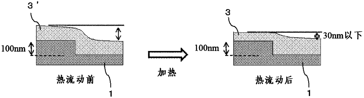
Method used
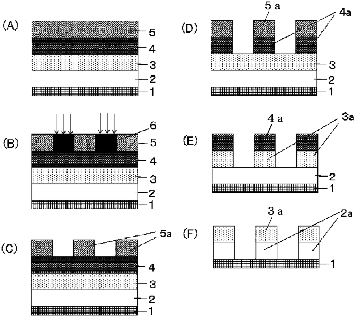
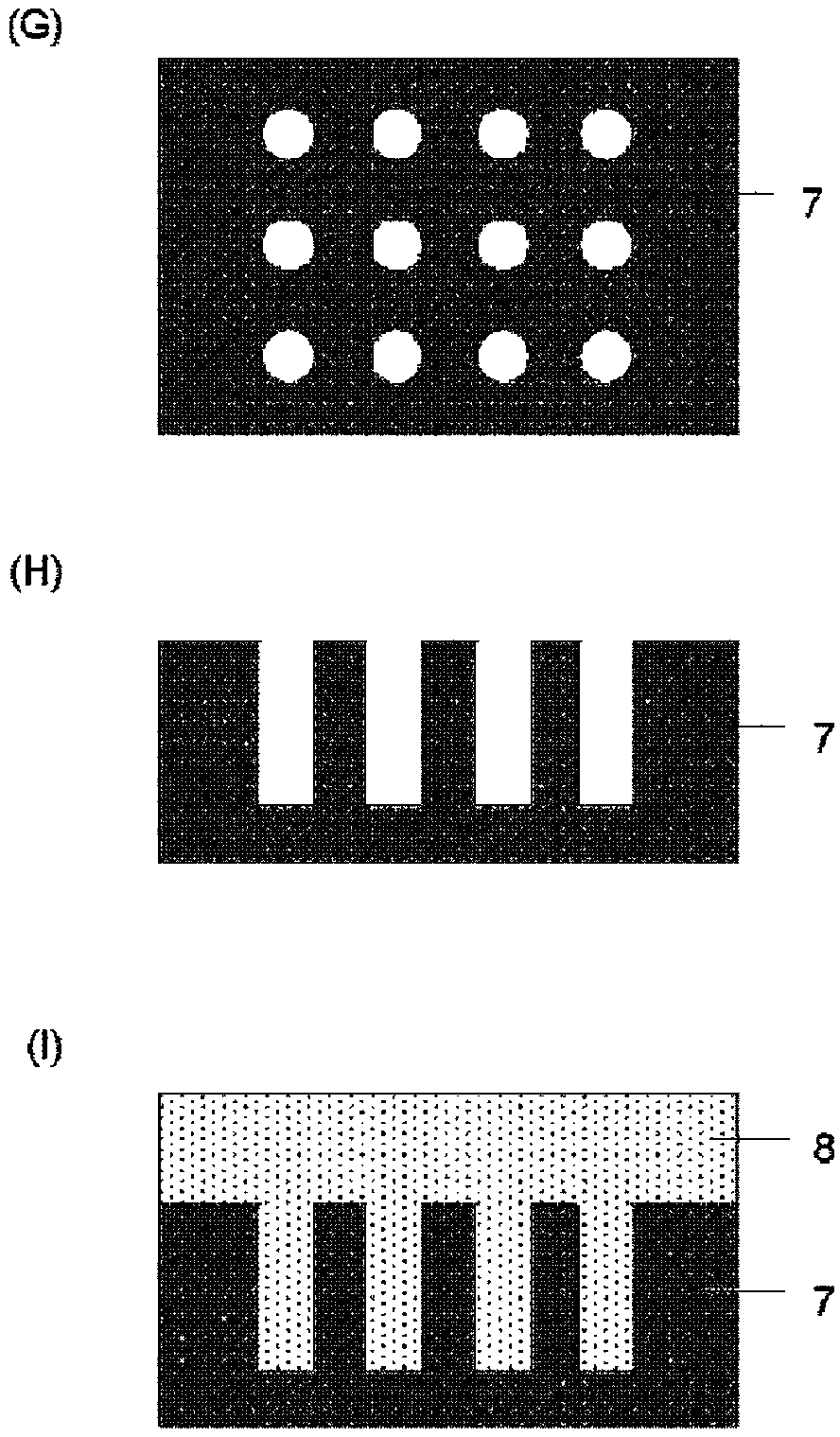
Image

Examples
preparation example Construction
[0114] [Preparation method of polymer]
[0115] As means for obtaining the polymer of the present invention, it can be obtained by the polycondensation reaction of the nitrogen-containing compound shown below with an aldehyde or a ketone. AR1, AR2, AR3, Y, R1 and R2 in the following formulas are as described above.
[0116] [chemical formula 16]
[0117]
[0118] The nitrogen-containing compound, aldehyde compound, and ketone compound used in these polycondensation reactions may be used alone or in combination of two or more. An aldehyde compound and a ketone compound may be used in combination. These can be appropriately selected and combined according to the required characteristics.
[0119] As the nitrogen-containing compound used in the polycondensation reaction, the following nitrogen-containing compounds can be specifically exemplified. Among them, indenocarbazole-type nitrogen-containing compounds are preferably used from the viewpoint of polymer heat resistance ...
Embodiment
[0226] Hereinafter, although a synthesis example, a comparative synthesis example, an Example, and a comparative example are shown, and this invention is demonstrated more concretely, this invention is not limited to this. In addition, as the molecular weight and degree of dispersion, polystyrene-equivalent weight average molecular weight (Mw) and number average molecular weight (Mn) were obtained by gel permeation chromatography (GPC) using tetrahydrofuran as an eluent, and the degree of dispersion was obtained.
Synthetic example
[0227] Synthesis Example Synthesis of Compounds for Organic Film Forming Composition
[0228] In the synthesis of the compounds (A1) to (A22) for the composition for forming an organic film, the following compound group P: (P1) to (P12) and compound group Q: (Q1) to (Q5) were used. .
[0229] Compound Group P: Nitrogenous Compounds
[0230] [chemical formula 23]
[0231]
[0232] Compound Group Q: Aldehyde or Ketone Compounds
[0233] [chemical formula 24]
[0234]
[0235] Among them, a 37% formalin aqueous solution was used as the formaldehyde represented by (Q1).
PUM
| Property | Measurement | Unit |
|---|---|---|
| composition ratio | aaaaa | aaaaa |
| wavelength | aaaaa | aaaaa |
| boiling point | aaaaa | aaaaa |
Abstract
Description
Claims
Application Information
 - Generate Ideas
- Intellectual Property
- Life Sciences
- Materials
- Tech Scout
- Unparalleled Data Quality
- Higher Quality Content
- 60% Fewer Hallucinations
Browse by: Latest US Patents, China's latest patents, Technical Efficacy Thesaurus, Application Domain, Technology Topic, Popular Technical Reports.
© 2025 PatSnap. All rights reserved.Legal|Privacy policy|Modern Slavery Act Transparency Statement|Sitemap|About US| Contact US: help@patsnap.com