Gan-cdznte composite structural components with znte transition layer, application and preparation method thereof

A composite structure and transition layer technology, which is applied in the manufacture of electrical components, semiconductor devices, and final products, can solve the problems of low lattice mismatch and optical detection devices that have not yet been seen, so as to improve production efficiency and save production costs Effect

Active Publication Date: 2021-06-04
SHANGHAI UNIV
View PDF0 Cites 0 Cited by
  • Summary
  • Abstract
  • Description
  • Claims
  • Application Information

AI Technical Summary

Problems solved by technology

Moreover, the lattice constant of ZnTe is closer to CdZnTe than GaN, and the lattice mismatch is low. However, there have been no reports on the application of ZnTe to optical detection devices so far.

Method used


Image

  • Gan-cdznte composite structural components with znte transition layer, application and preparation method thereof
  • Gan-cdznte composite structural components with znte transition layer, application and preparation method thereof
  • Gan-cdznte composite structural components with znte transition layer, application and preparation method thereof

Examples


Embodiment 1

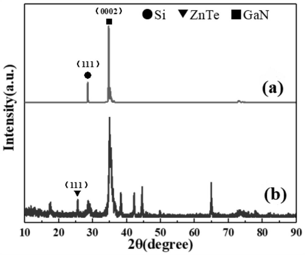
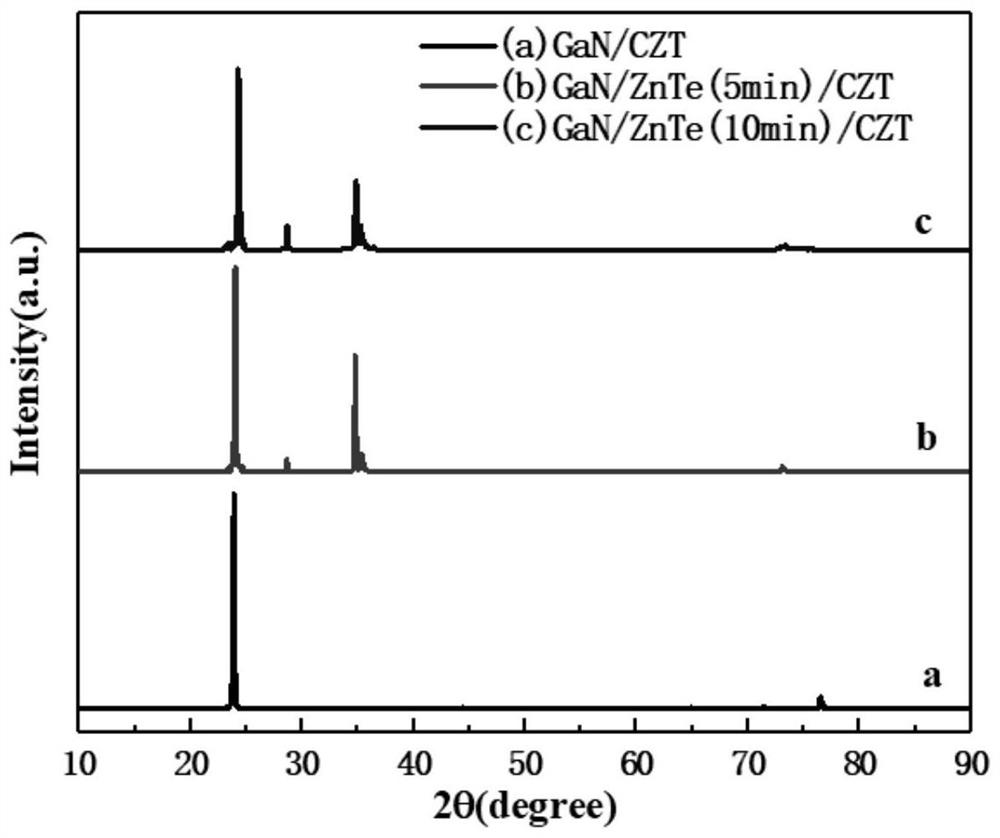
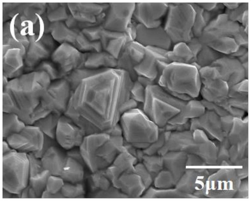
[0032]In this embodiment, a GaN-CdZnTe composite structural assembly with a ZnTe transition layer, first prepares a ZnTe transition layer on a GaN substrate to form a GaN-ZnTe composite substrate, and then forms a GaN-ZnTe composite substrate on the ZnTe transition layer of the GaN-ZnTe composite substrate The CdZnTe thin film is continuously grown on the surface to obtain a GaN-ZnTe-CdZnTe composite structural component combined with a CdZnTe transition layer and a GaN substrate. The deposited thickness of the ZnTe transition layer is 200nm. The thickness of the above-mentioned CdZnTe film is 20 μm, and the thickness of the GaN substrate is 500 nm.

[0033] In this embodiment, the preparation method of the GaN-CdZnTe composite structural component with a ZnTe transition layer in this embodiment, the steps are as follows:

[0034] a. Substrate pretreatment:

[0035] The GaN substrate with a thickness of 500nm was ultrasonically cleaned with acetone, alcohol, and deionized wa...

Embodiment 2

[0054] This embodiment is basically the same as Embodiment 1, especially in that:

[0055] In this embodiment, the preparation method of the GaN-CdZnTe composite structural component with a ZnTe transition layer of the present invention, the steps are as follows:

[0056] a. Substrate pretreatment:

[0057] The GaN substrate with a thickness of 500nm was ultrasonically cleaned with acetone, alcohol, and deionized water for 15 minutes respectively, and impurities and organic matter on the surface of the GaN substrate were washed away, dried with nitrogen, and then placed in a magnetron sputtering reaction chamber as Substrate spare;

[0058] b. Sputtering process of ZnTe transition layer:

[0059] Open the magnetron sputtering chamber, put the GaN substrate pretreated in step a into the chamber; turn on the mechanical pump, and when the vacuum degree of the chamber is lower than 5Pa, open the front valve, close the pre-pumping valve, and open the molecular Pump and high valv...


PUM

PropertyMeasurementUnit
thicknessaaaaaaaaaa
thicknessaaaaaaaaaa
thicknessaaaaaaaaaa

Abstract

The invention provides a GaN-CdZnTe composite structure component with a ZnTe transition layer, its application and its preparation method, based on a GaN / ZnTe substrate to grow a CdZnTe film and prepare a GaN / ZnTe / CdZnTe-based ultraviolet detector. The GaN provided by the invention The preparation method of / ZnTe / CdZnTe-based ultraviolet photodetector includes four main steps: substrate pretreatment, sputtering process of ZnTe transition layer, growth process of CdZnTe film, electrode fabrication of GaN / ZnTe / CdZnTe-based ultraviolet photodetector. The method of the present invention can rapidly grow a large-area, high-quality CdZnTe film on a GaN / ZnTe substrate, and the GaN / ZnTe substrate can ensure the use of GaN / ZnTe / CdZnTe-based ultraviolet light detectors in extreme environments, and the prepared composite The structure also has a strong photoresponse to ultraviolet light.

Description

technical field [0001] The invention relates to a semiconductor crystal composite material, its preparation process and application, in particular to a CdZnTe thin film device, its preparation process and application, and is applied in the technical fields of inorganic non-metallic material manufacturing and optical functional devices. Background technique [0002] Ultraviolet light refers to electromagnetic radiation with a wavelength range of 10nm-400nm, and its name comes from the fact that its spectrum is outside of violet light in visible light. The ultraviolet light in nature mainly comes from sunlight. When sunlight passes through the atmosphere, ultraviolet rays with a wavelength shorter than 290nm will be absorbed by the atmosphere. Most artificial ultraviolet light sources are gas arc discharges. With the development of science and technology, ultraviolet detection technology is more and more widely used in civilian and military fields. In the civil field, ultravi...

Claims


Application Information

Patent Timeline
Patent Type & Authority Patents(China)
IPC IPC(8): H01L31/0296H01L31/18H01L31/102
CPCH01L31/02966H01L31/102H01L31/1832H01L31/1836Y02P70/50
Inventor 沈悦孙佳豪徐宇豪顾峰黄健王林军
Owner SHANGHAI UNIV
Why Eureka
Try Eureka