Anti-visible and near-infrared memory pixels based on organic dyes
A pixel and memory technology, applied in the field of anti-visible light and near-infrared memory pixels, can solve the problems of near-infrared pixels not having anti-visible interference ability, misjudgment and misreading, etc.
- Summary
- Abstract
- Description
- Claims
- Application Information
AI Technical Summary
Problems solved by technology
Method used
Image
Examples
Embodiment 1
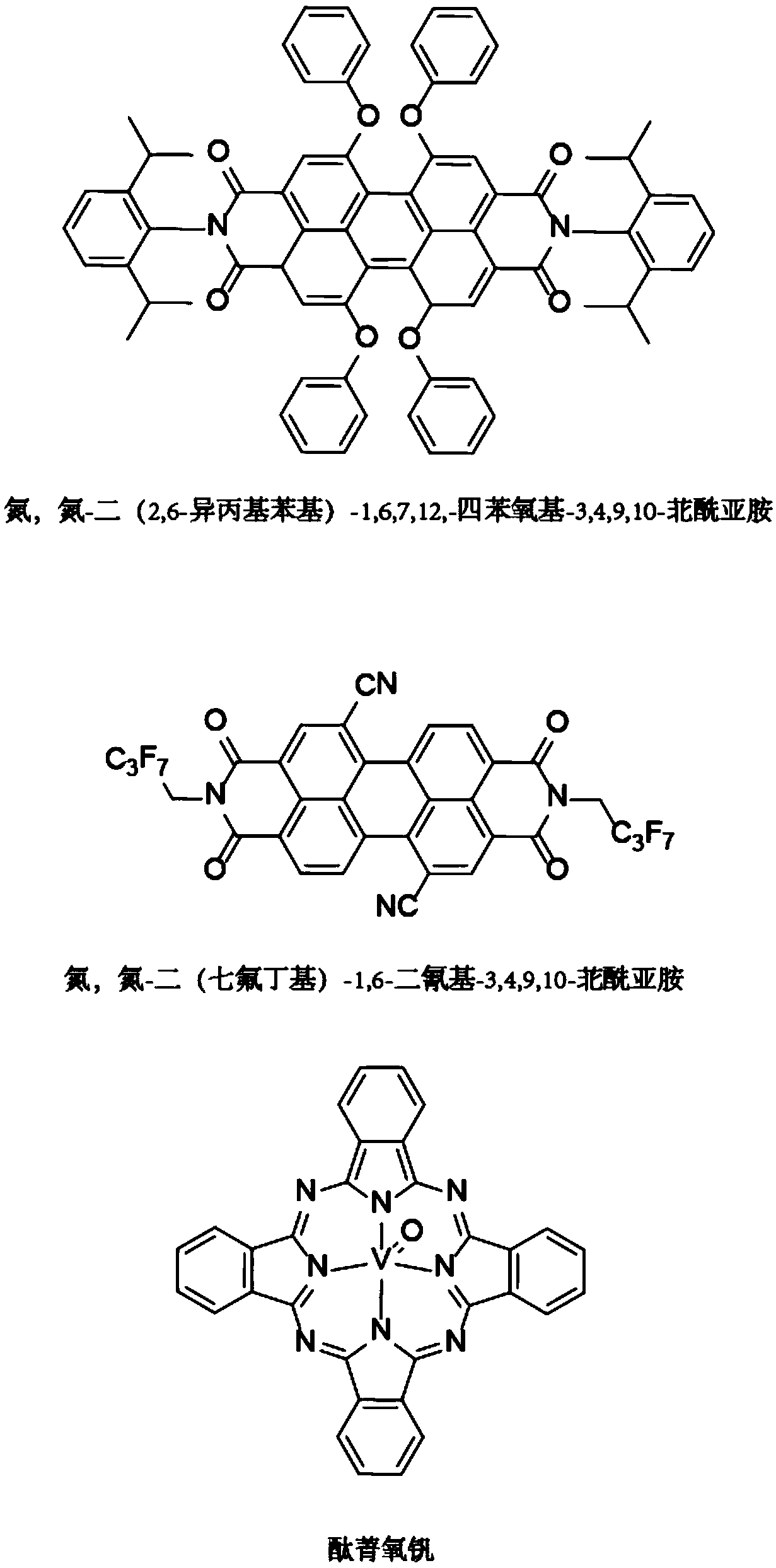
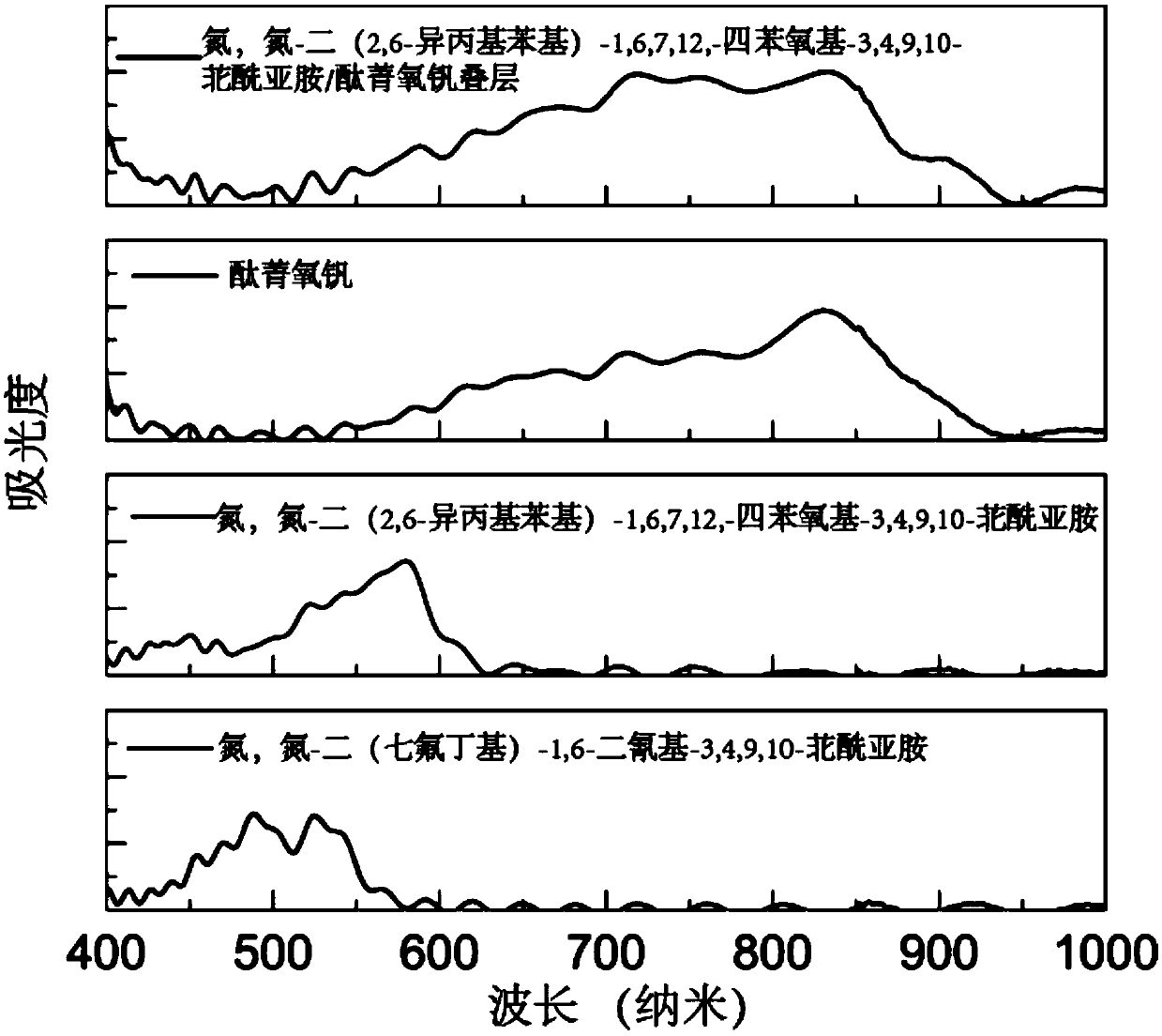
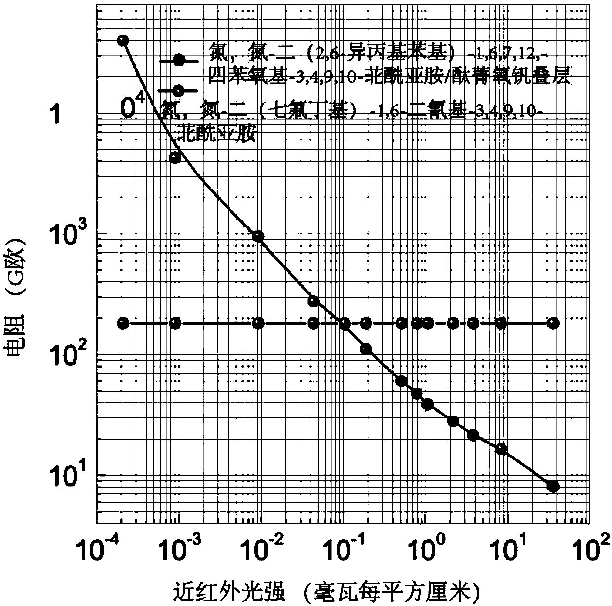
[0064] Example 1. Preparation of peryleneimide ROT300 / vanadyl phthalocyanine laminated photoresistor on polyethylene terephthalate film and its application in near-infrared light detection
[0065] 1) Clean the substrate
[0066] After the polyethylene terephthalate film was ultrasonically cleaned with detergent, secondary water, absolute ethanol, and isopropanol for 10 minutes, it was blown dry with nitrogen for use;
[0067] 2) Put the substrate obtained in step 1) into a vacuum coating machine, and first use the method of vacuum evaporation (vacuum degree is 3×10 -4 Pa, evaporation rate 1 angstrom / second) deposit a layer of gold with a thickness of 20 to 40 nanometers on the substrate as an electrode, and the channel length and width of the gold electrode are determined by a mask. Subsequently, vacuum thermal evaporation (vacuum degree of 3 × 10 -4 Pa, evaporation speed 1 Angstrom / second) perylene imide ROT300 with a thickness of 10 nanometers and a vanadyl phthalocyanine...
Embodiment 2
[0073] Example 2. Preparation of a photosensitive voltage divider constructed of all-organic conjugated molecules on a polyethylene terephthalate film
[0074] 1) The polyethylene terephthalate film was ultrasonically cleaned with detergent, secondary water, absolute ethanol, and isopropanol for 10 minutes in sequence, and then dried with nitrogen gas for use;
[0075] 2) Put the substrate obtained in step 1) into a vacuum coating machine, and first use the method of vacuum evaporation (vacuum degree is 3×10 -4 Pa, the evaporation rate is 1 angstrom / second) to deposit gold with a thickness of 20 to 40 nanometers on the substrate as an electrode, and the channel length and width of the gold electrode are determined by a mask. The gold electrode area covered by the heterojunction film has a channel length of 30 microns and a channel width of 1200 microns. Subsequently, the surface of the gold electrode in the designated photoresistor area was sequentially vacuum thermally evapo...
Embodiment 3
[0084] Example 3. Preparation of organic dye near-infrared memory pixels on polyethylene terephthalate film
[0085] 1) The polyethylene terephthalate film was ultrasonically cleaned with detergent, secondary water, absolute ethanol, and isopropanol for 10 minutes in sequence, and then blown dry with nitrogen for use;
[0086] 2) Put the substrate obtained in step 1) into a vacuum coating machine, and first use the method of vacuum evaporation (vacuum degree is 3×10 -4 Pa, evaporation speed 1 angstrom / second) deposits gold with a thickness of 20 to 40 nanometers on the substrate as the interdigital electrode, the channel length and width of the gold electrode are determined by the mask plate, the channel length is 50 microns, and the channel length is 50 microns. The track width was 4500 microns.
[0087] 3) Polyisoindigo-dithiophene (or polyisoindigo-dithiophene or polyisoindigo-dithiophene-isoindigo-dithiophene mixed polymer) o-dichloromethane on the surface of the film obt...
PUM
 Abstract
Description
Claims
Application Information


