Oxide semiconductor material of thin film transistor, thin film transistor and manufacturing method thereof
A technology of oxide semiconductor and thin film transistor, which is applied in semiconductor/solid-state device manufacturing, transistors, semiconductor devices, etc., can solve problems such as the inability to drive ultra-high-resolution display requirements, and achieve ultra-high-resolution display driving requirements, Stable performance and the effect of suppressing the generation of oxygen vacancies
- Summary
- Abstract
- Description
- Claims
- Application Information
AI Technical Summary
Problems solved by technology
Method used
Image
Examples
Embodiment 1
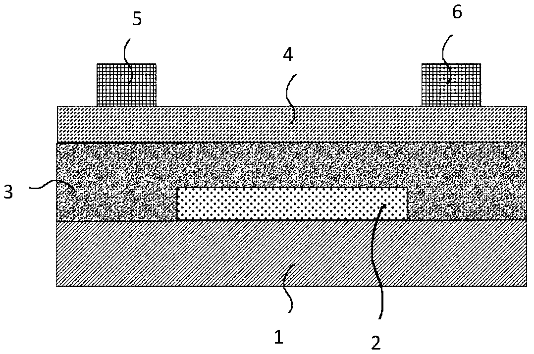
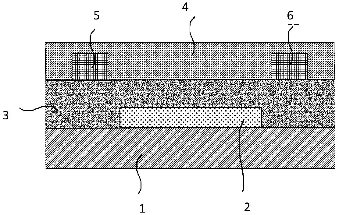
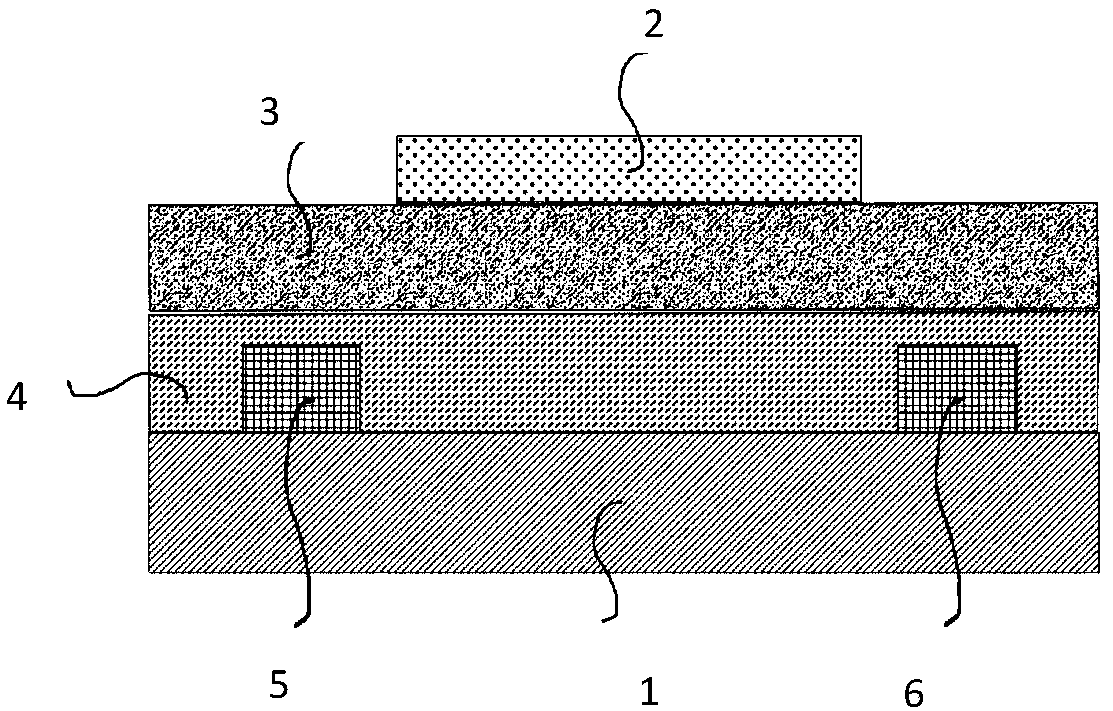
[0038] This embodiment adopts a bottom-gate top-contact thin film transistor structure, such as figure 1 shown.
[0039] A method for preparing a thin film transistor as described above, comprising the steps of:
[0040] (1) Prepare grid 2: manufacture a layer of Al-Nd thin film with a thickness of 300nm by sputtering on glass substrate 1, and then pattern it by photolithography to obtain grid 2;
[0041] (2) Preparation of insulating layer 3: Place the substrate 1 obtained by the above step (1) in the electrolyte as the anode, and the metal Pt as the cathode, and perform anodic oxidation to prepare Nd:Al 2 o 3 The insulating layer 3 has a thickness of 200nm;
[0042] (3) Preparation of active layer 4: prepare active layer 4 by magnetron sputtering, Nb 2 o 5 and In 2 o 3 The target is made by blending and pressing and sintering in a certain proportion to obtain the Nb-In-O target, wherein the mass percentage of the two is Nb 2 o 5 : In 2 o 3 = 5%: 95%, the Nb-In-O t...
Embodiment 2
[0046] This embodiment adopts a bottom-gate top-contact thin film transistor structure, such as figure 1 shown.
[0047] A method for preparing a thin film transistor as described above, comprising the steps of:
[0048] (1) Prepare grid 2: manufacture a layer of Al-Nd thin film with a thickness of 300nm by sputtering on glass substrate 1, and then pattern it by photolithography to obtain grid 2;
[0049] (2) Preparation of insulating layer 3: Place the substrate 1 obtained by the above step (1) in the electrolyte as the anode, and the metal Pt as the cathode, and perform anodic oxidation to prepare Nd:Al 2 o 3 The insulating layer 3 has a thickness of 200nm;
[0050] (3) Preparation of active layer 4: prepare active layer 4 by magnetron sputtering, Nb 2 o 5 and In 2 o 3 The target is made by blending and pressing and sintering in a certain proportion to obtain the Nb-In-O target, wherein the mass percentage of the two is Nb 2 o 5 : In 2 o 3 = 10%: 95%, the Nb-In-O ...
Embodiment 3
[0054] Performance tests were performed on the prepared TFT devices 1 and 2 in air. Figure 5 is the transfer characteristic curve measured by the thin film transistor prepared in Example 1, Figure 6 is the measured transfer characteristic curve of the thin film transistor prepared in Example 2, which is the relationship between the drain current and the gate voltage. Figure 5 and Figure 6 The test condition of the curve is: source voltage (V S ) is 0V, the drain voltage (V D ) is constant at 20V, the gate voltage (V G ) from -20V to 20V sweep, test the drain current (I D ).
[0055] From Figure 5 It can be seen that the thin film transistor in which the Nb-In-O material in Example 1 is used as the active layer has excellent electrical properties. Its Hall mobility reaches 36.3cm 2 V -1 the s -1 , turn-on voltage –5.1V, current switch ratio is 2.17×10 7 , to meet the driving requirements of ultra-high resolution display.
[0056] From Figure 6 It can be seen...
PUM
| Property | Measurement | Unit |
|---|---|---|
| Thickness | aaaaa | aaaaa |
| Thickness | aaaaa | aaaaa |
| Thickness | aaaaa | aaaaa |
Abstract
Description
Claims
Application Information
 - R&D Engineer
- R&D Manager
- IP Professional
- Industry Leading Data Capabilities
- Powerful AI technology
- Patent DNA Extraction
Browse by: Latest US Patents, China's latest patents, Technical Efficacy Thesaurus, Application Domain, Technology Topic, Popular Technical Reports.
© 2024 PatSnap. All rights reserved.Legal|Privacy policy|Modern Slavery Act Transparency Statement|Sitemap|About US| Contact US: help@patsnap.com


