A kind of multilayer cermet thin film with structural color and preparation method thereof
A multi-layer metal and ceramic thin film technology, applied in the field of nanomaterials, can solve the problems of lack of stability and mechanical properties, difficulty in large-scale preparation, high cost equipment requirements, etc., to achieve rich colors, low cost, and convenient adjustment of parameters Effect
- Summary
- Abstract
- Description
- Claims
- Application Information
AI Technical Summary
Problems solved by technology
Method used
Image
Examples
Embodiment 1
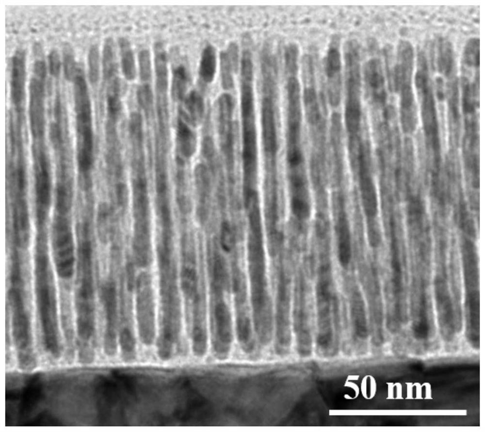
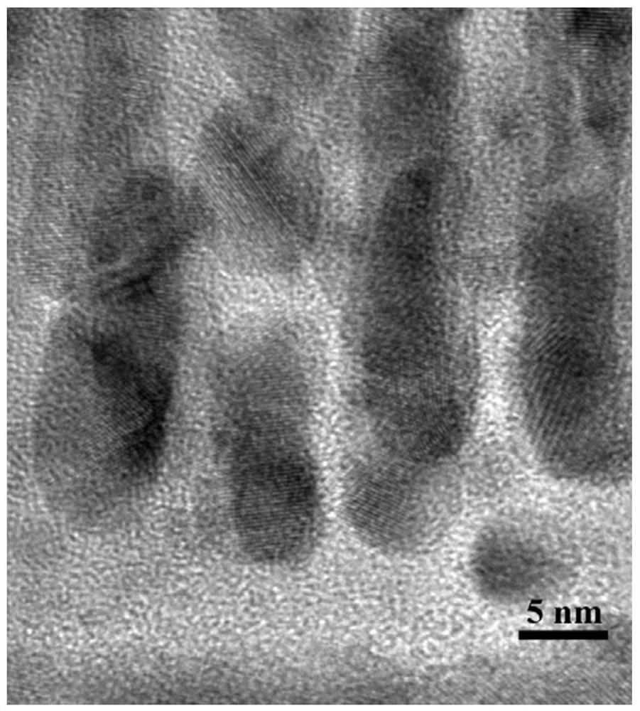
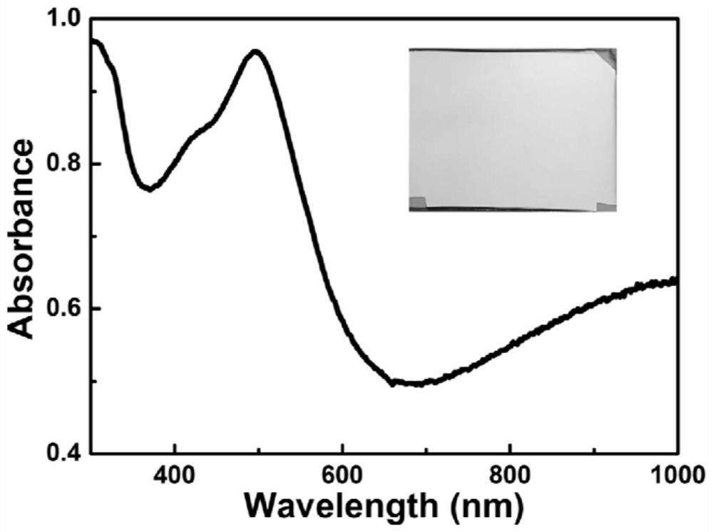
[0045] The silicon wafer and the quartz wafer were ultrasonically cleaned with acetone, ethanol and deionized water for 15 minutes respectively to remove surface pollutants; the cleaned silicon wafer was dried with nitrogen and fixed on the substrate tray; the tray was loaded into the magnetron In the deposition chamber of the sputtering equipment, pre-evacuate to 10 at the same time -4 Below Pa; the argon gas flow is introduced to keep the pressure of the deposition chamber at 0.4Pa, and the gold target and the silicon dioxide target are cleaned by radio frequency sputtering for 10 minutes, and the substrate is cleaned by applying a bias voltage for 5 minutes; after the etching and cleaning, adjust the deposition Chamber pressure to 0.3Pa, turn off the silicon dioxide target power, open the baffle in front of the gold target, start sputtering, adjust the sputtering power density of the gold target to 3.5W / cm 2 , deposit the metal layer, the deposition time is 25min. Turn off...
Embodiment 2
[0049] The silicon wafer and the quartz wafer were ultrasonically cleaned with acetone, ethanol and deionized water for 15 minutes respectively to remove surface pollutants; the cleaned silicon wafer was dried with nitrogen and fixed on the substrate tray; the tray was loaded into the magnetron In the deposition chamber of the sputtering equipment, pre-evacuate to 10 at the same time -4 Below Pa; the argon gas flow is introduced to keep the pressure of the deposition chamber at 0.4Pa, and the gold target and the silicon dioxide target are cleaned by radio frequency sputtering for 10 minutes, and the substrate is cleaned by applying a bias voltage for 5 minutes; after the etching and cleaning, adjust the deposition Chamber pressure to 0.3Pa, turn off the silicon dioxide target power, open the baffle in front of the gold target, start sputtering, adjust the power density of the gold target to 3.5W / cm 2 , deposit the metal reflective layer, and the deposition time is 25 minutes. ...
Embodiment 3
[0052] The PET sheet was ultrasonically cleaned with acetone, ethanol and deionized water for 15 minutes respectively to remove surface pollutants; the cleaned silicon wafer was dried with nitrogen and fixed on the substrate tray; the tray was loaded into the magnetron sputtering equipment deposition chamber while pre-evacuating to 10 -4 Below Pa; keep the pressure of the deposition chamber at 0.4Pa by introducing an argon gas flow, and clean the silver target with DC sputtering, and clean the aluminum oxide target with radio frequency sputtering for 20 minutes, and apply a bias voltage to clean the substrate for 5 minutes; After etching and cleaning, adjust the pressure of the deposition chamber to 0.25Pa, open the baffles in front of the silver target and the silicon dioxide target, start co-sputtering, and apply the substrate bias voltage at the same time. Among them, the sputtering power density of silver target and alumina target is 1.5W / cm 2 and 4.5W / cm 2 , the substra...
PUM
| Property | Measurement | Unit |
|---|---|---|
| thickness | aaaaa | aaaaa |
| thickness | aaaaa | aaaaa |
| thickness | aaaaa | aaaaa |
Abstract
Description
Claims
Application Information


