A method and device for growing microcrystalline silicon on the surface of a solar cell substrate

A technology for the surface of solar cells and substrates, applied in the directions of crystal growth, single crystal growth, single crystal growth, etc., can solve the problems of insufficient passivation effect and current loss on the whole surface, so as to improve cell efficiency and reduce energy costs , the effect of increasing the fill factor

Active Publication Date: 2021-07-16
JA SOLAR TECH YANGZHOU
View PDF4 Cites 0 Cited by
  • Summary
  • Abstract
  • Description
  • Claims
  • Application Information

AI Technical Summary

Problems solved by technology

Moreover, LPCVD mainly forms the entire surface of microcrystalline silicon, and the products formed by PECVD contain more amorphous silicon. Amorphous silicon is an amorphous product, which cannot achieve the required passivation effect.
If the entire surface of microcrystalline silicon is made on the front of the Topcon battery, the light absorption ratio of the microcrystalline silicon layer is strong, and the entire surface current will be lost.

Method used


Image

  • A method and device for growing microcrystalline silicon on the surface of a solar cell substrate
  • A method and device for growing microcrystalline silicon on the surface of a solar cell substrate

Examples


Embodiment 1

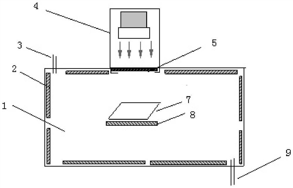
[0053] Such asfigure 1 The shown device for growing microcrystalline silicon on the surface of a solar cell substrate includes a closed cavity 1, a laser component 4, and the laser component 4 includes a laser, a scanning galvanometer and an optical component. The airtight cavity 1 is in the shape of a cuboid, and the laser is located outside the airtight cavity 1, and is specifically arranged in such as figure 1 On the outside of the top surface of the airtight cavity 1 shown, a transparent window 5 made of quartz is provided on an outer wall of the airtight cavity 1, that is, in the middle of the top surface. The transparent window 5 is rectangular, and there is a corresponding scanning window above the transparent window. The vibrating mirror and the laser, the laser and the scanning vibrating mirror are integrated and fixed in a shield fixedly connected with the airtight cavity 1 . Inside the airtight cavity 1 there is a stage 7 for placing the solar cell substrate, and th...

Embodiment 2

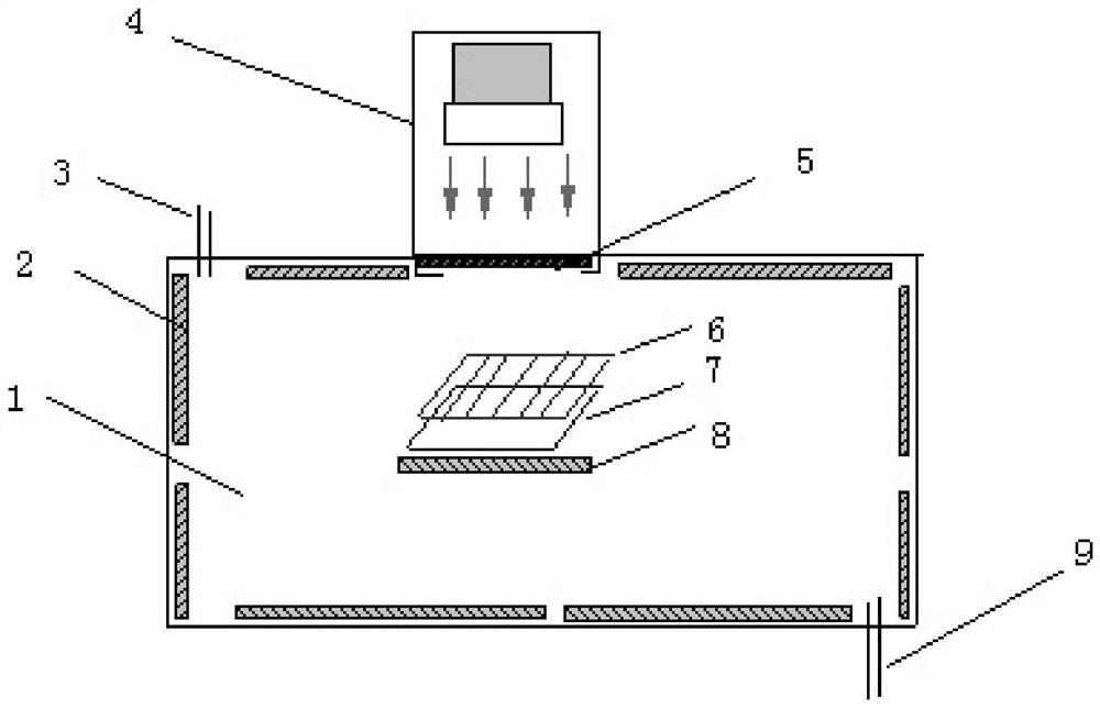
[0064] The difference between this embodiment and Embodiment 1 is that, as figure 2 As shown, in the device for growing microcrystalline silicon on the surface of a solar cell substrate in this embodiment, the laser emitted by the laser is a surface light source, and a mask 6 is set above the solar cell substrate, and the mask is positioned between the transparent window 5 and the solar cell substrate placed on the stage 7. The mask is a special component for solar cell manufacturing. For its structure and principle, please refer to the invention patent application number 201310505063.8 "New mask and use of ion implanter". The common one is graphite mask, which can be square or round as a whole. Etc., a part of the mask plate is hollowed out, and the hollowed out shape can be a hole shape, a stripe shape or a grid shape. Other implementation steps of this embodiment are the same as those of Example 1, wherein the graphite mask can be replaced by a ceramic mask or a quartz ma...


PUM

PropertyMeasurementUnit
thicknessaaaaaaaaaa

Abstract

The invention discloses a method and a device for growing microcrystalline silicon on the surface of a solar cell substrate. The method includes the following steps: S1: placing the solar cell substrate into a closed cavity, and a transparent window is arranged on the closed cavity; S2: making the closed cavity into a vacuum environment; S3: to the closed cavity Passing silane into the cavity; S4 : irradiating the solar cell substrate with a laser through the transparent window by a laser located outside the closed cavity, so as to decompose the silane to generate microcrystalline silicon. According to this method, a selected target area on the surface of the solar cell substrate is irradiated with laser light. In the irradiated area, the silane is decomposed due to the high temperature, thereby generating microcrystalline silicon, and in the unirradiated area, Because the temperature is low, microcrystalline silicon is not substantially generated, and as a result, local microcrystalline silicon can be generated.

Description

technical field [0001] The invention relates to solar cell manufacturing technology, in particular to a method and device for growing microcrystalline silicon on the surface of a solar cell substrate. Background technique [0002] The tunnel oxide passivated contact (Tunnel Oxide Passivated Contact, Topcon for short) solar cell (cell for short), originates from the Topcon technology developed by the Fraunhofer Institute in Germany. In the Topcon technology, first a layer of ultra-thin silicon oxide is chemically prepared on the back of the cell, and then a thin layer of doped silicon is deposited, which together form a passivation contact structure. Because of the tunneling effect of the ultra-thin oxide layer and the passivation effect of microcrystalline silicon, the Topcon cell has a high open circuit voltage and fill factor, so it has a high conversion efficiency, and is a research hotspot in the solar cell industry at present. [0003] Microcrystalline silicon is a kin...

Claims


Application Information

Patent Timeline
Patent Type & Authority Patents(China)
IPC IPC(8): H01L31/18H01L21/02C23C16/04C23C16/24C23C16/48C30B29/06C30B30/00
CPCC23C16/042C23C16/24C23C16/483C30B29/06C30B30/00H01L21/02532H01L21/02595H01L21/0262H01L31/1824Y02E10/545Y02P70/50
Inventor 段光亮蒋秀林卢林
Owner JA SOLAR TECH YANGZHOU
Why Eureka
Try Eureka