

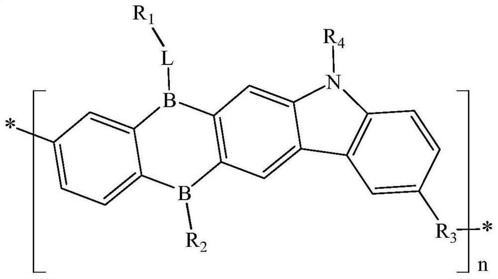
Polymer, display panel and display device
A technology for display panels and polymers, applied in the directions of luminescent materials, chemical instruments and methods, electric solid devices, etc., to achieve the effects of improving solubility, weakening charge transfer, and increasing energy levels
- Summary
- Abstract
- Description
- Claims
- Application Information
AI Technical Summary
Problems solved by technology
Method used
Image

Examples
Embodiment 1
[0102] Synthesis of Polymer M1
[0103] The synthetic route of polymer M1 is shown below.
[0104]
[0105] The synthesis steps of polymer M1 are as follows:
[0106]
[0107] In a 200ml stuffy tank, sequentially add compound A (5.12, 20mmol), compound B (9.14g, 20mmol), anhydrous toluene 100ml and BBr 3 (10g, 40mmol), start stirring, heat up to 120°C and stir for 12h. After the reaction is over, slowly add 70ml of ice water to quench, then add dichloromethane (100ml×3) to extract the reaction solution, and then use saturated brine (100ml ×2) Washing, liquid separation, drying, filtration, spin-drying of the filtrate, and recrystallization using toluene / ethanol to obtain white solid C with a yield of 80%.
[0108] MALDI-TOF: 604.99
[0109] 1 H NMR(400MHz,C):δ7.81(s,3H),7.66(s,2H),7.36(s,3H),7.30(d,J=12.2Hz,2H),4.15(s,2H), 1.73(s,2H),1.29(d,J=27.9Hz,10H),0.89(s,3H).
[0110] 13 C NMR (100MHz, CDCl 3 ): δ167.29(s), 143.65(s), 140.34(s), 135.67(s), 134.81(s), 133.8...
Embodiment 2
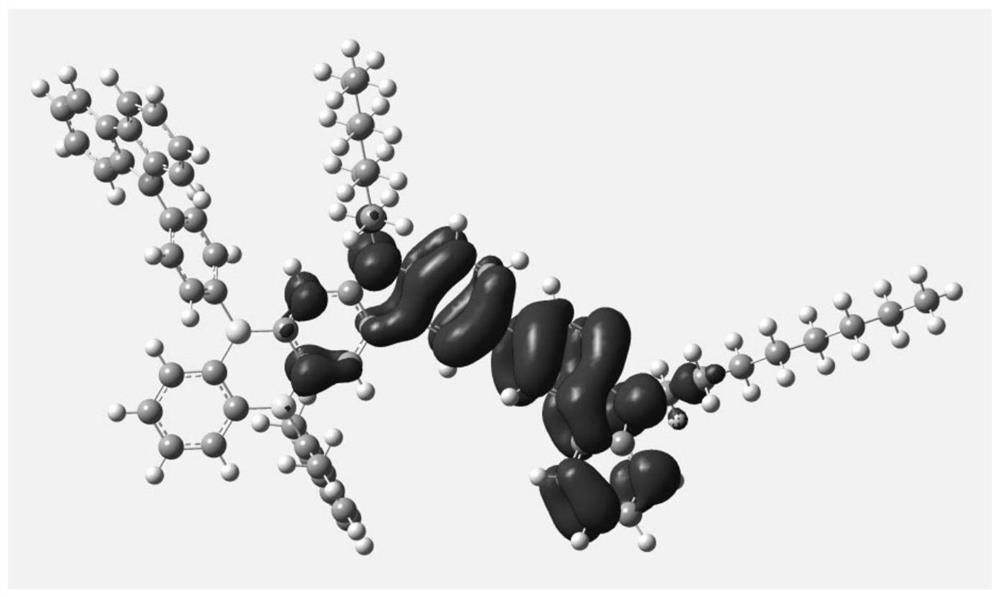
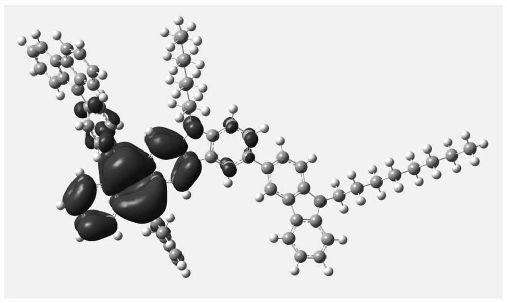
[0122]The electroluminescent properties of the exemplary polymeric materials M1, M2, M3 and M4 described herein were simulated using Gaussian software.
[0123] figure 2 with image 3 The HOMO and LUMO energy level diagrams of exemplary polymer M1 of the present invention are shown. It can be clearly seen from the figure that the HOMO and LUMO of the polymer molecule are respectively arranged on the donor unit and the acceptor unit, which realizes the complete separation of HOMO and LUMO, which helps to reduce the energy difference between systems △E ST , so as to improve the inverse intersystem crossing ability.
[0124] Table 1 Parameters of four representative polymers
[0125]
Embodiment 3
[0127] Taking M1 as an example, it is used as a fluorescent dopant (guest material), and the classic polymer material PVK is used as the host material, and the doped device structure is designed:
[0128] ITO (100 nm) / PEDOT:PSS (60 nm) / PVK:M1 (40 nm, 5%) / TmPyPb (50 nm) / LiF (0.5 nm) / Al (100 nm).
[0129] Similarly, the design comparison device structure is as follows:
[0130] ITO (100 nm) / PEDOT:PSS (60 nm) / PVK:BCzVBi (40 nm, 5%) / TmPyPb (50 nm) / LiF (0.5 nm) / Al (100 nm).
[0131] Fabrication of OLED devices
[0132] The structure of the OLED device is as Image 6 As shown, the brief description of its production process is as follows: put the substrate 1 into a rotary washing and drying machine, first wash it with deionized water and flush it with nitrogen, and then treat it with ultraviolet light for 20 minutes to completely remove the residual oil on the surface and improve the anode 2 (the material is ITO) work function, using a combination of high and low speed, two-way s...
PUM
| Property | Measurement | Unit |
|---|---|---|
| glass transition temperature | aaaaa | aaaaa |
| thermal decomposition temperature | aaaaa | aaaaa |
| tensile strength | aaaaa | aaaaa |
Abstract
Description
Claims
Application Information