A Photonic Crystal Fiber Sensor with Pentagonal Arrangement
A technology of photonic crystal fiber and pentagon, which is applied in the direction of cladding fiber, optical waveguide and light guide, instrument, etc., can solve the problems of low sensing detection sensitivity, single sensor structure, not easy to prepare, etc., and achieve simple design structure, high sensitivity, easy to prepare effects
- Summary
- Abstract
- Description
- Claims
- Application Information
AI Technical Summary
Problems solved by technology
Method used
Image
Examples
Embodiment 1
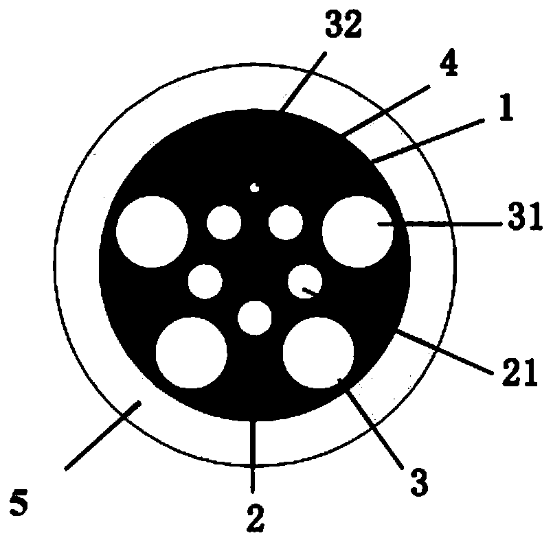
[0059] This embodiment adopts figure 1 The photonic crystal fiber sensor shown in a pentagonal arrangement is called the first sensor for short.
[0060] Figure 4 for figure 1 Schematic diagram of the front view of the three-dimensional structure. The photonic crystal fiber of the present invention is composed of base material 1 , cladding air holes and gold nanowires 4 . Figure 4 Among them, the air hole layout is a pentagon with the inner and outer layers inverted, the air hole 2 in the inner layer is smaller, and the air hole 3 in the outer layer is larger in size; the uppermost air hole in the cladding is the main sensing channel, and all of them are filled with the liquid to be measured; Gold nanowires 4 are fixed at the bottom of the inner wall of the second air hole 32, which is used as an induction material for surface plasmon resonance effect; the air hole is circular.
[0061] Dislocation fusion splicing of the solid traditional single-mode optical fiber and th...
Embodiment 2
[0075] This embodiment provides a D-shaped photonic crystal fiber sensor prepared based on photonic crystal fiber side polishing technology, referred to as the second sensor.
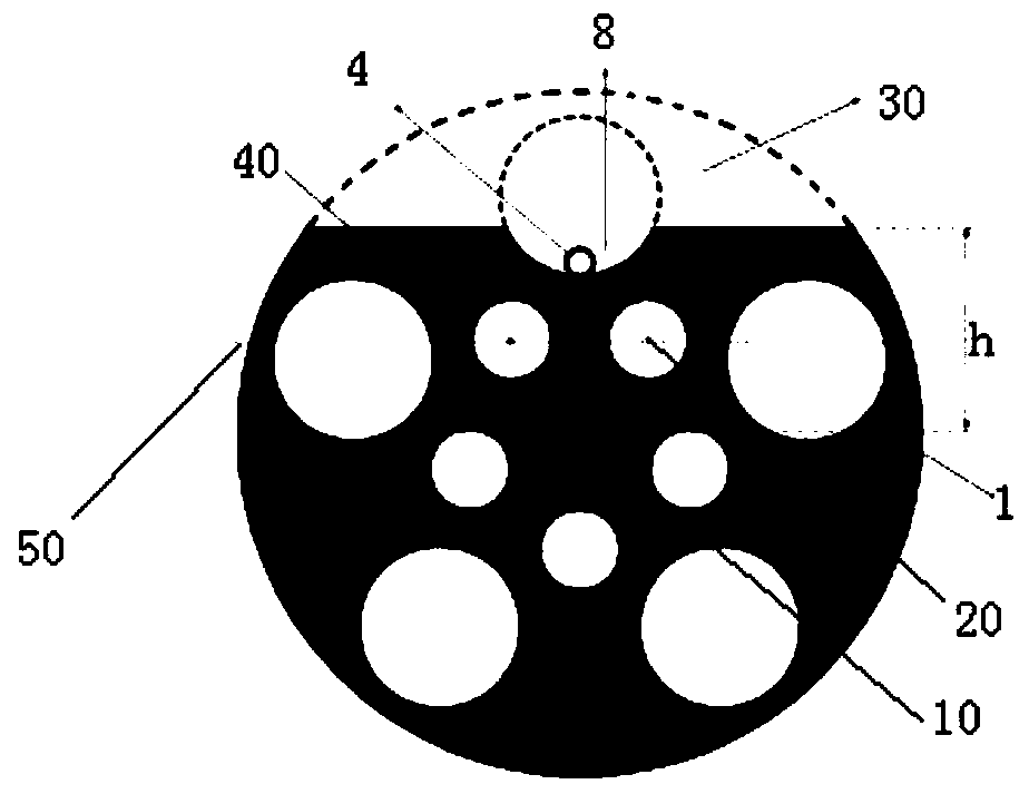
[0076] Figure 9a It is a schematic diagram of the optical fiber end face structure when the second air hole of the present invention is circular, which is the structure given in Example 1; Figure 9b for in Figure 9a Basically, the schematic diagram of the D-shaped optical fiber end face structure when the second air hole formed by side polishing is fan-shaped, and the polishing depth of the optical fiber is required to be h=3 μm or h=4 μm, which is the optical fiber structure used in Example 2.
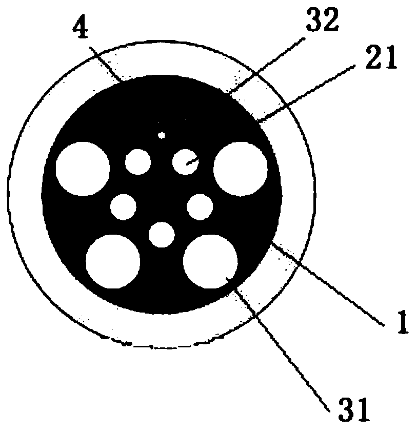
[0077] Combine below Figure 2b brief introduction Figure 9b The preparation method of optical fiber sensor. Specifically: firstly, the optical fiber preforms are arranged into a pentagonal structure by stacking method, and then drawn into Figure 9a The second air hole shown is a circular photonic cry...
PUM
| Property | Measurement | Unit |
|---|---|---|
| diameter | aaaaa | aaaaa |
| refractive index | aaaaa | aaaaa |
Abstract
Description
Claims
Application Information


