Method of manufacturing semiconductor device

A manufacturing method and semiconductor technology, which are applied in the fields of semiconductor/solid-state device manufacturing, electrical components, circuits, etc., can solve the problems of lack of convenience of sacrificial films, and achieve the effect of simplifying the manufacturing process

Pending Publication Date: 2019-04-30
TOKYO ELECTRON LTD
View PDF1 Cites 0 Cited by
  • Summary
  • Abstract
  • Description
  • Claims
  • Application Information

AI Technical Summary

Problems solved by technology

[0008] Therefore, in the future manufacturing process of semiconductor manufacturing equipment, it can be said that the current sacrificial film lacks convenience.

Method used


Image

  • Method of manufacturing semiconductor device
  • Method of manufacturing semiconductor device
  • Method of manufacturing semiconductor device

Examples


no. 1 Embodiment approach >

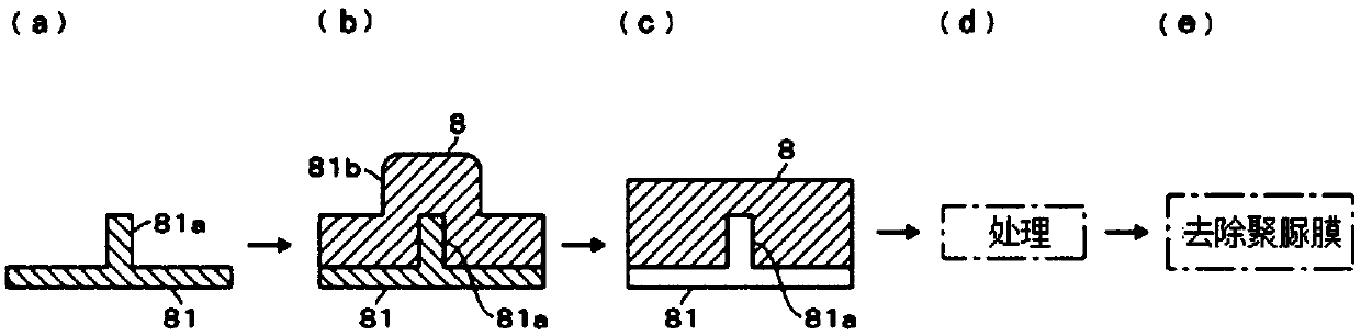
[0072] The first embodiment is a method of forming a sacrificial film on a level difference substrate having a level difference formed on the surface, for example, a silicon wafer subjected to predetermined film formation processing and etching, and an example thereof is shown in figure 1 . figure 1 In the example, the substrate 81 ( figure 1 (a)) Polyurea film 8 ( figure 1 (b)).

[0073] For polyurea membranes, for example, such as Figure 5 As shown, it can be produced by copolymerization using isocyanate and amine. R is, for example, an alkyl group (straight-chain or cyclic alkyl) or an aryl group, and n is an integer of 2 or more.

[0074] As the isocyanate, for example, an alicyclic compound, an aliphatic compound, an aromatic compound or the like can be used. As alicyclic compounds, for example, such as Figure 6 As shown in (a), 1,3-bis(isocyanatomethyl)cyclohexane (H6XDI) can be used. In addition, as aliphatic compounds, for example, such as Figure 6 As sh...

no. 2 Embodiment approach >

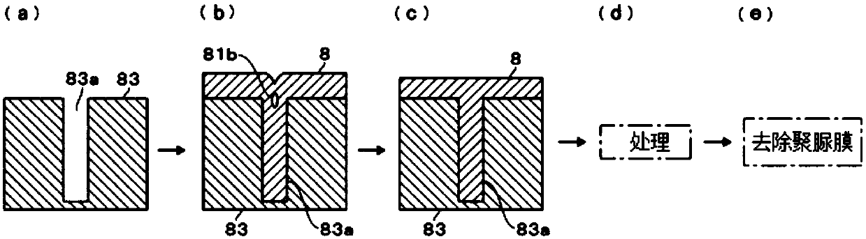
[0096] The second embodiment is a method of forming a sacrificial film of a protective film on a surface having a concave portion such as a narrow and deep hole or groove, and an example thereof is shown in image 3 . image 3 In an example, the substrate 83 ( image 3 (a)) Polyurea film 8 ( image 3 (b)). The hole diameter or groove width of the concave portion 83 a is, for example, 100 nm to 10 nm, and the aspect ratio is, for example, 2 or more. When the polyurea film 8 is formed on the substrate 83 having such a concave portion 83a, before the polyurea film 8 is completely embedded in the concave portion 83a, the entrance of the concave portion 83a is blocked, and as a result, voids (voids or seams) are formed in the concave portion 83a. ) 83b. In addition, depressions are formed on the surface of the polyurea film 8 at positions corresponding to the recesses 83 a.

[0097] If the void 83b is formed in the concave portion 83a, the polyurea film 8 may not be able to fu...

no. 3 Embodiment approach >

[0102] The third embodiment is a method of permeating a polyurea film into a porous low dielectric constant film to form a sacrificial film as a protective film, an example of which is shown in Figure 4 . Figure 4 In the example described in the first embodiment, for example, the low dielectric constant film 20 ( Figure 4 (a)) upper film-forming polyurea film 8 ( Figure 4 (b)). The SiOC film is formed, for example, by CVD by plasmating DEMS (diethoxymethylsilane). For the film formation of the polyurea film 8, for example, when isocyanate gas and amine gas are alternately supplied into the low dielectric constant film 20, the gas permeates into the pores 21 in the low dielectric constant film 20 to form a polyurea film. A state where the film 8 is laminated on the low dielectric constant film 20 while polyurea (indicated by a blackened portion) enters the hole portion 21 .

[0103] At this time, the embedding of polyurea into the hole 21 is insufficient, that is, a voi...


PUM


Abstract

The invention provides a method of manufacturing a semiconductor device, which is capable of easily adjusting a shape and film amount of a sacrificial film when manufacturing a semiconductor device using the sacrificial film, which can contribute to simplification of processes. A raw material for polymerization is supply to the surface of a substrate, thereby forming the sacrificial film composedof a polymer (polyurea film 8) with urea bonds. As an example of a film forming method, the sacrificial film can be generated by means of isocyanate and amine through copolymerization. For an example,the two raw materials are alternately supplied to the surface in a gas state in a vacuum atmosphere. Through heating the sacrificial film, depolymerization of one part occurs, thereby forming a monomer, and further polymerization is performed through cooling. Therefore, the section shape of the sacrificial film can be changed, and the height difference part of the sacrificial film on a height difference substrate can be flattened, or a state with a clearance in a recessed part is changed to a state with embedded polyurea. Furthermore the thickness of the sacrificial film can be adjusted (reduced) through depolymerization.

Description

technical field [0001] The present invention relates to a technique of manufacturing a semiconductor device using a sacrificial film. Background technique [0002] In the manufacturing process of a semiconductor device, a film called a sacrificial film is sometimes used. The sacrificial film is a film that is used in the manufacturing process and removed in the middle and is not included in the semiconductor device as a product. As the sacrificial film, there are: an organic film used to form a reticle corresponding to the resist mask on the lower layer side of the mask, and an organic film used as an intermediate film for separating trenches and via holes in dual damascene Wait. [0003] In addition, as a sacrificial film, as described in Patent Document 1, it is also known that the pores of a porous low dielectric constant film on the substrate are embedded in advance, and after the low dielectric constant film is etched, the substrate is etched. PMMA (acrylic resin) or...

Claims


Application Information

Patent Timeline
IPC IPC(8): H01L21/02C08G71/02
CPCC08G71/02H01L21/02H01L21/02282H01L21/0271H01L21/3105H01L21/31058H01L21/31144H01L21/67115H01L21/02271H01L21/02118H01L21/76808H01L21/76826H01L21/76811H01L21/76865H01L21/7688H01L21/76864H01L21/76837H01L21/76828H01L21/02205
Inventor 山口达也新纳礼二野泽秀二藤川诚
Owner TOKYO ELECTRON LTD
Why Eureka
Try Eureka