Ultrathin metal based transparent conductive film

A transparent conductive film, ultra-thin metal technology, applied in conductive layers on insulating carriers, metal material coating process, ion implantation plating, etc., can solve the problem of insufficient film adhesion, poor thermal stability, and poor oxidation resistance. and other problems, to achieve the effect of excellent anti-scratch stability, improved humidity and heat stability, and improved stability

Active Publication Date: 2019-05-21
NINGBO INST OF MATERIALS TECH & ENG CHINESE ACADEMY OF SCI
View PDF5 Cites 4 Cited by
  • Summary
  • Abstract
  • Description
  • Claims
  • Application Information

AI Technical Summary

Problems solved by technology

However, the application of the AZO / Ag / AZO DMD film is not particularly ideal, and there are a series of problems such as incomplete protection of the silver film and insufficient film adhesion, which are specifically reflected in: (1) Poor resistance to humidity and heat, oxygen in the outside air , Water easily penetrates the AZO layer and diffuses to the silver film, resulting in the oxidation failure of the silver film; (2) The oxidation resistance in the air is poor, after a period of time in the air, the silver film is easy to oxidize and agglomerate, and white spots appear on the surface of the film , thereby affecting the photoelectric properties of the film; (3) poor thermal stability during high-temperature heat treatment; (4) poor adhesion between the AZO layer and the silver film, and film surface contact and friction during handling will cause film scratches, affect the quality of the film surface

Method used


Image

  • Ultrathin metal based transparent conductive film
  • Ultrathin metal based transparent conductive film
  • Ultrathin metal based transparent conductive film

Examples


Embodiment 1

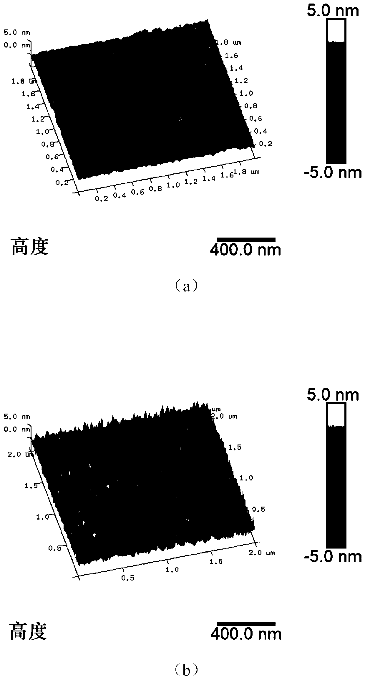
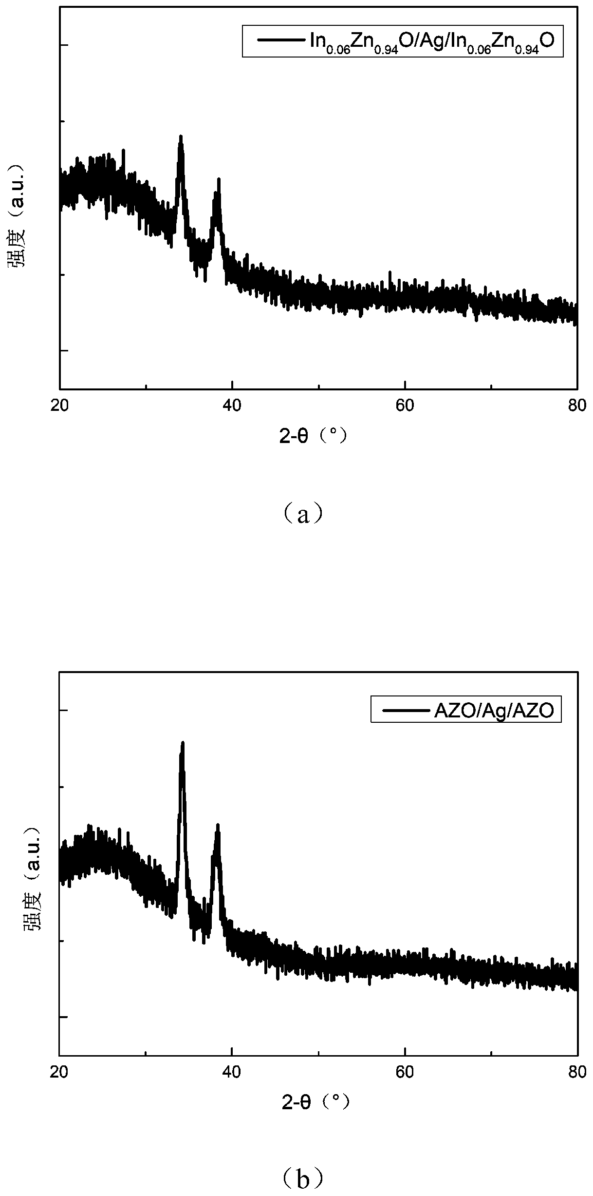
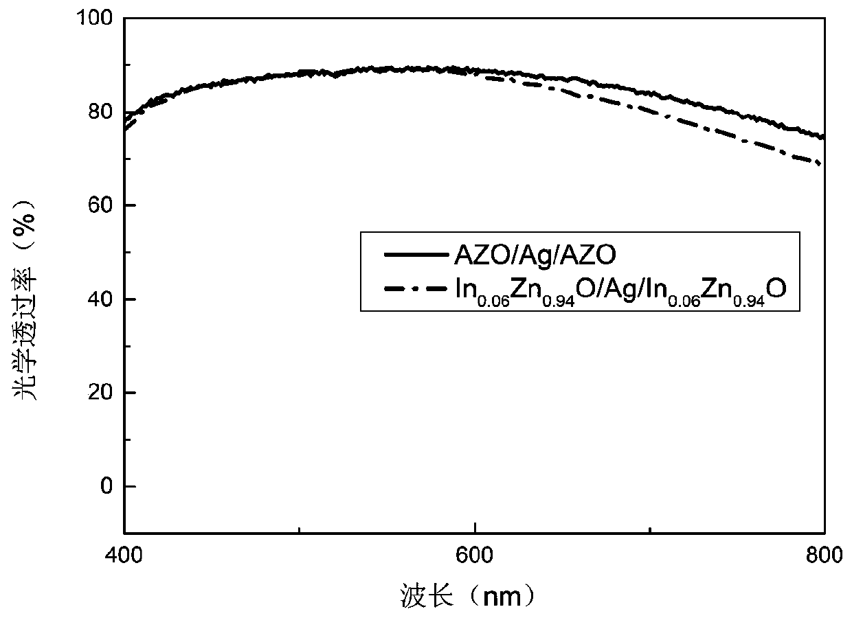
[0022] The ultra-thin metal-based transparent conductive film of embodiment 1 includes a bottom dielectric layer, an ultra-thin metal layer and a top dielectric layer arranged in sequence from bottom to top, the ultra-thin metal layer is a silver layer, the top dielectric layer and the bottom The chemical composition of the dielectric layer is In x Zn 1-x O, where In is the doping element, and In is In 2 o 3 Incorporated into ZnO in the form of In x Zn 1-x O, x = 0.06.

[0023] In embodiment 1, the thickness of the bottom dielectric layer and the top dielectric layer are both 40 nm, and the thickness of the ultra-thin metal layer is 10 nm.

[0024] In Example 1, both the bottom dielectric layer and the top dielectric layer are made of In-doped 2 o 3 The ZnO target material is deposited by radio frequency magnetron sputtering at room temperature. The specific process is: when the background vacuum degree is less than 6.8×10 -4 In the state of Pa, radio frequency magnetr...

Embodiment 2

[0031] The ultra-thin metal-based transparent conductive film of embodiment 2 includes a bottom dielectric layer, an ultra-thin metal layer and a top dielectric layer arranged in sequence from bottom to top, the ultra-thin metal layer is a silver layer, the top dielectric layer and the bottom The chemical composition of the dielectric layer is Mg x Zn 1-x O, where Mg is a doping element, and Mg is doped into ZnO in the form of MgO to obtain Mg x Zn 1-x 0,x=0.24.

[0032] In embodiment 2, the thickness of the bottom dielectric layer and the top dielectric layer are both 40 nm; the thickness of the ultra-thin metal layer is 10 nm.

[0033] In Example 2, both the bottom dielectric layer and the top dielectric layer are obtained by radio frequency magnetron sputtering deposition of MgO-doped ZnO targets at room temperature. The specific process is as follows: when the background vacuum degree is less than 6.8×10 -4 In the state of Pa, radio frequency magnetron sputtering film ...

Embodiment 3

[0037] The ultra-thin metal-based transparent conductive film of embodiment 3 includes a bottom dielectric layer, an ultra-thin metal layer and a top dielectric layer arranged in sequence from bottom to top, the ultra-thin metal layer is a silver layer, the top dielectric layer and the bottom The chemical composition of the dielectric layer is Gd x Zn 1-x O, where Gd is a doping element, and Gd is doped into ZnO in the form of GdO to obtain Gd x Zn 1-x O, x=0.01.

[0038] In embodiment 3, the thickness of the bottom dielectric layer and the top dielectric layer are both 45nm; the thickness of the ultra-thin metal layer is 8nm.

[0039] In embodiment 3, both the bottom dielectric layer and the top dielectric layer are made of Gd-doped 2 o 3 The ZnO target material is deposited by radio frequency magnetron sputtering at room temperature. The specific process is: when the background vacuum degree is less than 6.8×10 -4 In the state of Pa, radio frequency magnetron sputterin...


PUM

PropertyMeasurementUnit
surface roughnessaaaaaaaaaa
thicknessaaaaaaaaaa
thicknessaaaaaaaaaa

Abstract

The invention discloses an ultrathin metal based transparent conductive film. The ultrathin metal based transparent conductive film comprises a bottom dielectric layer, an ultrathin metal layer and atop dielectric layer which are sequentially arranged from bottom to top, wherein the ultrathin metal layer is a silver layer; the bottom dielectric layer and the top dielectric layer both comprise thechemical components of MxZn1-xO; the average surface roughness of the bottom dielectric layer is 0.1-0.3 nm; M is a doped element and is any one of Mg, In and Gd; x is the mass ratio of the doping amount of M to the total quantity of M and Zn, and x is 0.005-0.5. The transparent conductive film is provided with a three-layer structure; compared with existing common transparent conductive films with the same structures, the ultrathin conductive film has the advantages that the high-temperature stability, the hydrothermal stability, the chemical stability, the in-air stability, the scraping resisting stability and other performances are greatly improved on the premise that the average optical transmission rate is not less than 80% under the wavelength of 400-800nm, and the film sheet resistance is not beyond 7 ohms / sq; and the application demands of a plurality of flexible photoelectric appliances can be met.

Description

technical field [0001] The invention belongs to the field of flexible photoelectric films, in particular to a transparent conductive film based on ultra-thin metal. Background technique [0002] In recent years, facing the needs of wearable devices, thin-film optoelectronic devices have gradually developed in the direction of flexibility, and the demand for flexible transparent conductive films has become increasingly urgent. At present, indium tin oxide (ITO) film is the most commonly used transparent conductive film in the market. Due to the limitation of the brittleness of the oxide itself, it has been difficult to meet the needs of flexible optoelectronic devices. Therefore, flexible transparent conductive film products that can replace ITO must be the basic material for future flexible optoelectronic products, and even more strategic materials for flexible optoelectronic products. [0003] Among the flexible transparent conductive film materials that have been studied ...

Claims


Application Information

Patent Timeline
Patent Type & Authority Applications(China)
IPC IPC(8): C23C14/35C23C14/08C23C14/18H01B5/14
Inventor 宋伟杰王肇肇李佳黄金华杨晔许君君
Owner NINGBO INST OF MATERIALS TECH & ENG CHINESE ACADEMY OF SCI
Why Eureka
Try Eureka