White light LED preparation method and white light LED device
A technology of LED devices and white light, applied in semiconductor devices, electrical components, circuits, etc., can solve the problems of large difference in refractive index, enhanced total reflection effect at the interface, unfavorable LED light output, etc., achieve simple process and improve light extraction efficiency Effect
- Summary
- Abstract
- Description
- Claims
- Application Information
AI Technical Summary
Problems solved by technology
Method used
Image
Examples
Embodiment 1
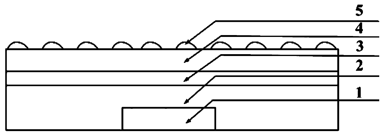
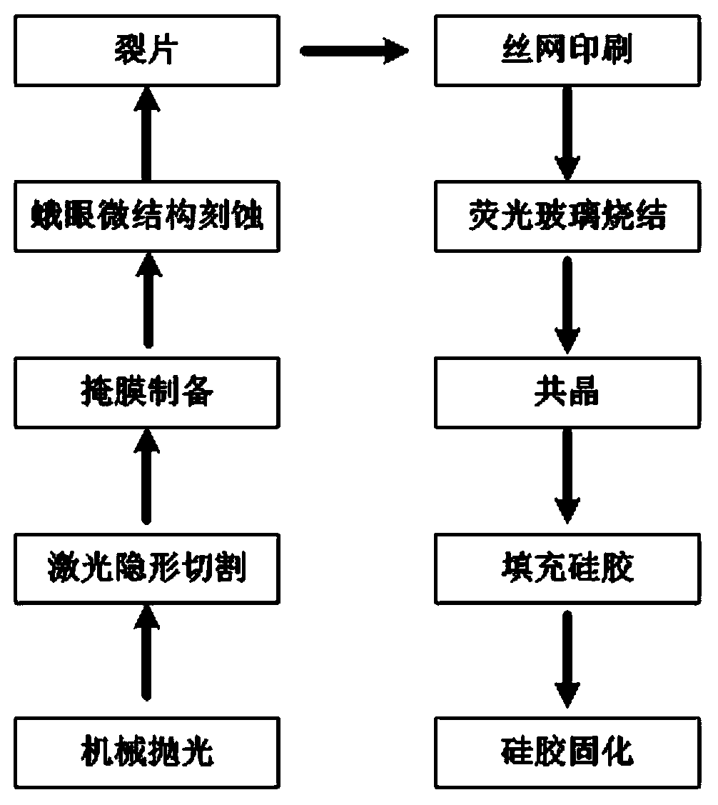
[0028] The sapphire sheet is chemically mechanically polished to a thickness of 200 μm, the surface of the sapphire is cut using a laser, mask preparation, etching, and splitting are performed to obtain a sapphire sheet 4 with a moth-eye microstructure array 5 on the upper surface.
[0029] The red phosphor CaAlSN 3 :Eu 2+ , green phosphor Ba 2 MgSi 2 o 7 :Eu 2+ Mix with glass powder according to the ratio of 1:2:7, then pour into organic solvent and stir well.
[0030] A phosphor layer 3 was prepared on the lower surface of the sapphire sheet by screen printing, and sintered in an air furnace at 600°C for 30 minutes to obtain a phosphor glass with a moth-eye microstructure array.
[0031] The ultraviolet LED chip 1 with a light emission wavelength of 395nm is eutectic in the middle of a 3.2mm*3.2mm AlN ceramic substrate, and silica gel 2 is coated on the top of the chip and the ceramic substrate, and a fluorescent glass with a thickness of 20μm is placed on the silica ge...
Embodiment 2
[0033] The sapphire sheet is chemically mechanically polished to a thickness of 200 μm, the surface of the sapphire is cut using a laser, mask preparation, etching, and slivers are performed to obtain a sapphire sheet with a moth-eye microstructure array on the upper surface.
[0034] The red phosphor CaAlSN 3 :Eu 2+ , green phosphor Ba 2 MgSi 2 o 7 :Eu 2+ Mix with glass powder according to the ratio of 1:2:7, then pour into organic solvent and stir well.
[0035] A phosphor layer was prepared on the lower surface of the sapphire sheet by screen printing, and sintered in an air furnace at 600°C for 30 minutes to obtain a phosphor glass with a moth-eye microstructure array.
[0036] Put the ultraviolet LED chip eutectic with a light emission wavelength of 395nm in the middle of a 3.2mm*3.2mm AlN ceramic substrate, coat silica gel on the top of the chip and the ceramic substrate, place a fluorescent glass with a thickness of 48μm on top of the silica gel, and vacuum at 120°...
Embodiment 3
[0038] The sapphire sheet is chemically mechanically polished to a thickness of 200 μm, the surface of the sapphire is cut using a laser, mask preparation, etching, and slivers are performed to obtain a sapphire sheet with a moth-eye microstructure array on the upper surface.
[0039] The red phosphor CaAlSN 3 :Eu 2+ , green phosphor Ba 2 MgSi 2 o 7 :Eu 2+ Mix with glass powder according to the ratio of 1:2:7, then pour into organic solvent and stir well.
[0040] A phosphor layer was prepared on the lower surface of the sapphire sheet by screen printing, and sintered in an air furnace at 600°C for 30 minutes to obtain a phosphor glass with a moth-eye microstructure array.
[0041] Put the ultraviolet LED chip eutectic with a light emission wavelength of 395nm in the middle of the 3.2mm*3.2mm AlN ceramic substrate, coat the silica gel on the chip and the ceramic substrate, place the fluorescent glass with a thickness of 84μm on the silica gel, and vacuum at 120℃ Conditio...
PUM
| Property | Measurement | Unit |
|---|---|---|
| thickness | aaaaa | aaaaa |
| thickness | aaaaa | aaaaa |
| height | aaaaa | aaaaa |
Abstract
Description
Claims
Application Information


