Thin film flip structure Micro-LED chip transferred by adhesive layer, and preparation method thereof

A thin-film flip-chip and adhesive layer technology, which is applied to semiconductor devices, electrical components, circuits, etc., can solve the problems of uneven heating of epitaxial wafers, small laser spot area, and local heating, so as to improve light extraction efficiency and improve Photoelectric properties, the effect of enhancing adhesion

Active Publication Date: 2020-12-01
JIANGXI ZHAO CHI SEMICON CO LTD
View PDF4 Cites 6 Cited by
  • Summary
  • Abstract
  • Description
  • Claims
  • Application Information

AI Technical Summary

Problems solved by technology

The emission wavelength of a typical blue LED chip is about 450nm. Due to the high refractive index of the GaN material (about 2.5), when the light emitted from the active layer of the LED chip propagates at the GaN / air interface, the wavelength is shortened to about 180nm. At this time, the wavelength is much smaller than The size of the roughened structure, so the traditional roughening method limits the further improvement of the light extraction efficiency of the LED chip
[0005] In addition, the current removal of sapphire substrates mainly uses laser lift-off technology. The laser is incident on the interface between the substrate and the epitaxial layer from the side of the sapphire substrate. Large stress is caused, the spot area of ​​the laser is small, and it can only heat the local position, resulting in uneven heating of the epitaxial wafer during the peeling process, thus forming defects such as pitting and cracks on the epitaxial wafer, which will damage and reduce the Micro-LED device. photoelectric performance
[0006] In addition, the outgoing light of the traditional LED chip will be totally reflected at the interface of the side walls of the chip, and oscillate between the two side walls until it is absorbed by the chip and converted into heat energy, which greatly reduces the light extraction efficiency of the chip; and, the traditional LED In order to facilitate the lateral diffusion of current in the chip, a thick current blocking layer is often set up, but this will easily cause the ITO transparent conductive layer and metal electrodes deposited on the current blocking layer to be faulted at the sidewall of the current blocking layer, which will lead to LED The forward voltage of the chip increases sharply, which reduces the photoelectric performance of the LED chip

Method used


Image

  • Thin film flip structure Micro-LED chip transferred by adhesive layer, and preparation method thereof
  • Thin film flip structure Micro-LED chip transferred by adhesive layer, and preparation method thereof
  • Thin film flip structure Micro-LED chip transferred by adhesive layer, and preparation method thereof

Examples


Embodiment Construction

[0050] The specific embodiments of the thin-film flip-chip micro-LED chip with the adhesive layer transferred and the preparation method thereof according to the present invention will be described in detail below with reference to the accompanying drawings.

[0051]

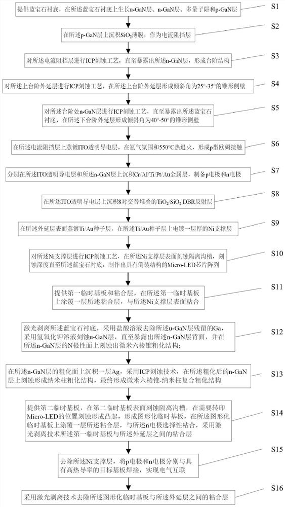
[0052] Such as Figures 1 to 8 As shown, the preparation method of the thin-film flip-chip structure Micro-LED chip with adhesive layer transfer provided in this embodiment includes the following steps:

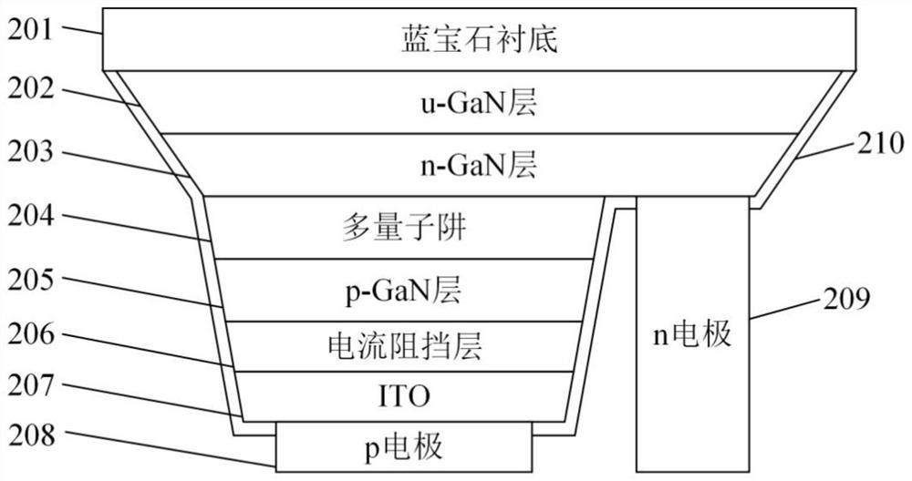
[0053] S1: Provide a sapphire substrate 201, grow an epitaxial layer 200 on the sapphire substrate 201, and the epitaxial layer 200 is an undoped u-GaN layer 202, a Si-doped n-GaN layer 203, and an InGaN / GaN layer from bottom to top. The multiple quantum wells 204 and the Mg-doped p-GaN layer 205; specifically, the epitaxial layer 200 is grown by MOCVD technology, and the light emission wavelength of the epitaxial layer 200 is 450nm.

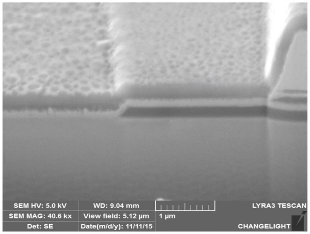
[0054] S2: Deposit SiO on the p-GaN layer by PECVD technology 2 thin fil...


PUM

PropertyMeasurementUnit
thicknessaaaaaaaaaa
thicknessaaaaaaaaaa
thicknessaaaaaaaaaa

Abstract

The invention provides a thin film flip structure Micro-LED chip transferred by an adhesive layer, and a preparation method thereof. The light extraction efficiency of the chip can be effectively improved. The preparation method comprises the following steps: growing an epitaxial layer on a substrate; depositing a current blocking layer; etching to form a frustum-shaped first frustum-shaped epitaxial layer and a frustum-shaped second frustum-shaped epitaxial layer; forming a p electrode and an n electrode; depositing a plurality of pairs of alternately stacked DBR reflecting layers; evaporating a Ti/Au seed layer on the surface of the epitaxial layer, and electroplating a thick Ni support layer on the seed layer; etching ane isolation groove to manufacture a chip array with a flip structure; etching a micron hexagonal pyramid coarsening structure on the N polar surface of the n-GaN layer; further etching to obtain a nanopillar coarsened structure; coating the graphical temporary substrate with a bonding layer, and selectively bonding with the surface of the n electrode; removing the Ni support layer, and respectively welding the p electrode and the n electrode to the target substrate; and removing the bonding layer to obtain the transferred chip.

Description

technical field [0001] The invention belongs to the technical field of semiconductor light-emitting diodes, and in particular relates to a micro-LED chip with a thin-film flip-chip structure transferred by an adhesive layer and a preparation method thereof. [0002] technical background [0003] Micro-LED has the advantages of high resolution, long life, small size, high brightness and low power consumption. It has important application value in the fields of high-resolution display, optical communication, micro-projector and wearable electronics. The focus of attention of technologically powerful countries. Thin-film flip-chip structure Micro-LEDs are flip-chip-bonded to target substrates with high thermal conductivity through metal bumps, and low-resistance p-type ohmic contact electrodes with high reflectivity are used to reflect the outgoing light of the active layer to avoid horizontal structures The light absorption phenomenon of the metal electrode on the top of the M...

Claims


Application Information

Patent Timeline
Patent Type & Authority Applications(China)
IPC IPC(8): H01L33/48H01L33/32H01L33/06H01L33/20H01L33/38H01L33/14
CPCH01L33/06H01L33/14H01L33/20H01L33/32H01L33/38H01L33/48
Inventor 周圣军宫丽艳万辉唐斌
Owner JIANGXI ZHAO CHI SEMICON CO LTD
Why Eureka
Try Eureka