Plasma nano-structure assisted femtosecond laser nano-manufacturing method and system

A femtosecond laser and nanostructure technology, applied in the field of femtosecond laser nanoprocessing, can solve the problems of limited cost of processing materials, high processing environment requirements, and difficulty in breaking through the optical diffraction limit, and achieve a wide range of processing materials and simple processing technology Easy-to-do, easy-to-control effects

Inactive Publication Date: 2019-06-07
XI AN JIAOTONG UNIV
View PDF7 Cites 16 Cited by
  • Summary
  • Abstract
  • Description
  • Claims
  • Application Information

AI Technical Summary

Problems solved by technology

[0008] In order to solve the problems existing in the above-mentioned micro-nano processing methods such as difficulty in breaking through the optical diffraction limit, high requirements on the processing environment, limited processing materials and high cost, the present invention proposes a femtosecond laser nano-processing method based on plasma nanostructure assistance , using the localized surface plasmon resonance enhancement (LSPR) of femtosecond laser-induced plasmonic nanomaterials, a method that can implement laser direct writing processing on the surface of various materials in free space

Method used


Image

  • Plasma nano-structure assisted femtosecond laser nano-manufacturing method and system
  • Plasma nano-structure assisted femtosecond laser nano-manufacturing method and system
  • Plasma nano-structure assisted femtosecond laser nano-manufacturing method and system

Examples


Embodiment Construction

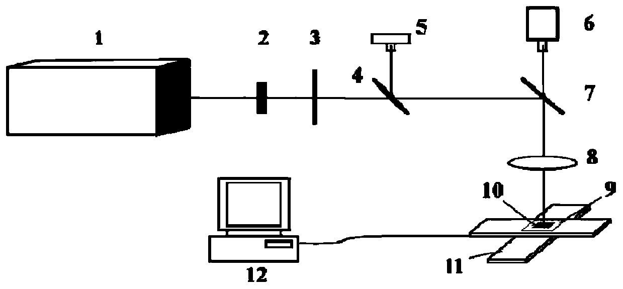
[0052] The present invention will be further described in detail below in conjunction with the accompanying drawings and specific embodiments.

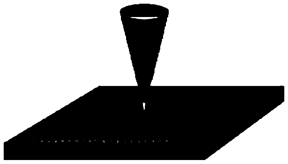
[0053] The invention focuses the femtosecond laser on the plasma nanostructure, induces local surface plasmon resonance thermal field enhancement in the plasma nanostructure through the femtosecond laser, and forms a local field enhancement beyond the optical diffraction limit on the surface of the material to be processed, realizing Diffraction-limited-scale nanofabrication of substrate materials. Any material including hard and brittle materials can be surface-arrayed and patterned with ultra-high-resolution nanofabrication in free space to obtain specific processing patterns.

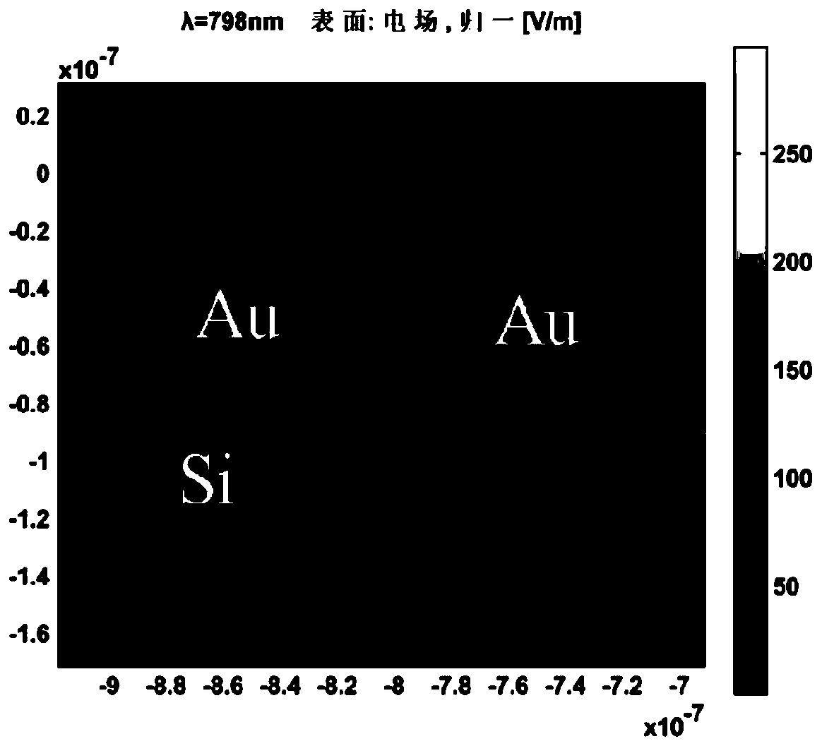
[0054] In this embodiment, the Au nano-grating structure is used as the plasmonic nano-structure, and the Si material is used as the material to be processed, and is realized through the following steps:

[0055] 1) Select the Si material to be processed, a...


PUM

PropertyMeasurementUnit
thicknessaaaaaaaaaa
widthaaaaaaaaaa

Abstract

The invention provides a plasma nano-structure assisted femtosecond laser nano-manufacturing method and system and belongs to the field of laser micronano-structure processing. Through the plasma nano-structure assisted femtosecond laser nano-manufacturing method and system, the problems that the optical diffraction limit is hard to break through during conventional laser precision machining, a hard and brittle material is hard to machine, the requirements for the machining environment are high, the cost is high and machining is hard to implement in the air environment are solved. According tothe method, through LSPR enhancement of a plasma nano-structure is motivated through femtosecond laser to generate a space height localized patterning optical near field beyond the optical diffraction limit on the surface of the material to be machined, and the material is subjected to area arrayed and patterned ultrahigh resolution nano-machining. Through the method, the limitation of the optical diffraction limit of a traditional machining method can broken through, and wide-range and high-precision parallel machining is realized. The method has the characteristics that the range of the machining material is wide, free special machining is realized, the cost is low, and the method is simple and easy to implement.

Description

technical field [0001] The invention belongs to the technical field of nanostructure preparation, and in particular relates to a plasma nanostructure-assisted femtosecond laser nanoprocessing method, which directly processes the surfaces of various materials including hard and brittle materials with arrayed and patterned structures. Background technique [0002] The micro-nano processing technology on the surface of materials involves national defense and military industry, aerospace industry, biomedicine, environmental health and safety and other major issues related to national human development, especially in the field of semiconductor electronics. With the continuation and breakthrough of Moore's Law, The micro-nano processing technology of semiconductor materials, especially the surface of silicon materials, needs to be developed urgently. [0003] At the same time, with the continuous advancement of science and technology, various micro-nano processing methods have dev...

Claims


Application Information

Patent Timeline
Patent Type & Authority Applications(China)
IPC IPC(8): B23K26/352B23K26/00B23K26/064
Inventor 杜广庆陈烽董彦宏杨青
Owner XI AN JIAOTONG UNIV
Why Eureka
Try Eureka