Diamond-based field effect transistor with low work function conductive gate and preparation method thereof

A low work function, conductive gate technology, applied in semiconductor/solid-state device manufacturing, semiconductor devices, circuits, etc., can solve the problem of reducing the surface channel carrier concentration and mobility, sacrificing the external transconductance of the source and drain maximum current of the device, etc. problems, to achieve the effect of realizing the characteristics of normally-off devices, ensuring the ability of current passing, and ensuring the ability of current transport

Active Publication Date: 2019-06-18
XI AN JIAOTONG UNIV
View PDF4 Cites 1 Cited by
  • Summary
  • Abstract
  • Description
  • Claims
  • Application Information

AI Technical Summary

Problems solved by technology

Existing normally-off devices are usually realized by converting part of the hydrogen termination to oxygen termination, partial desorption of surface adsorbates, and compensation of the oppositely charged dielectric layer, which will reduce the surface channel carrier concentration and migration rate, sacrificing the maximum source-drain current and external transconductance performance of the device

Method used


Image

  • Diamond-based field effect transistor with low work function conductive gate and preparation method thereof
  • Diamond-based field effect transistor with low work function conductive gate and preparation method thereof
  • Diamond-based field effect transistor with low work function conductive gate and preparation method thereof

Examples


Embodiment 1

[0065] A method for preparing a normally-off surface channel diamond field-effect transistor with a low work function conductive gate according to an embodiment of the present invention includes the following steps:

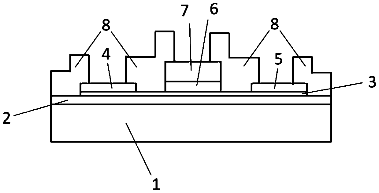
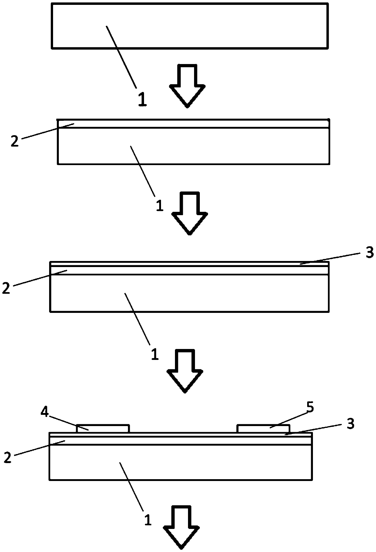
[0066] 1) The diamond substrate 1 grown by high temperature and high pressure (HPHT) technology is cleaned successively by using the standard cleaning process for diamond substrates, followed by inorganic and organic cleaning, and blown dry with nitrogen gas for later use.

[0067] 2) Deposit a single crystal diamond film 2 on the cleaned diamond substrate using microwave plasma vapor chemical deposition (MPCVD), the plasma power is 1kW, the chamber pressure is 100Torr, and the total gas flow is 500sccm, and the obtained single crystal diamond The thickness of the film is 0.1μm, the resistivity is greater than 100MΩ cm, the root mean square (RMS) surface roughness is 0.5nm, and the half-peak width of the Raman curve is about 3cm -1 , XRD rocking curve half width ...

Embodiment 2

[0074] A method for preparing a normally-off surface channel diamond field-effect transistor with a low work function conductive gate according to an embodiment of the present invention includes the following steps:

[0075] 1) The diamond substrate 1 grown by the vapor phase epitaxy (CVD) technique is successively cleaned inorganically and organically by using a standard diamond substrate cleaning process, and blown dry with nitrogen gas for later use.

[0076] 2) Deposit a single crystal diamond film 2 on the cleaned diamond substrate using microwave plasma vapor chemical deposition (MPCVD), the plasma power is 1kW, the chamber pressure is 100Torr, and the total gas flow is 500sccm, and the obtained single crystal diamond The thickness of the film is 10μm, the resistivity is greater than 100MΩ cm, the root mean square (RMS) surface roughness is 0.5nm, and the half-peak width of the Raman curve is about 3cm -1 , XRD rocking curve half width less than 50arcsec.

[0077] 3) Co...

Embodiment 3

[0083] A method for preparing a normally-off surface channel diamond field-effect transistor with a low work function conductive gate according to an embodiment of the present invention includes the following steps:

[0084] 1) The diamond substrate 1 grown by high temperature and high pressure (HPHT) technology is cleaned successively by using the standard cleaning process for diamond substrates, followed by inorganic and organic cleaning, and blown dry with nitrogen gas for later use.

[0085] 2) Deposit a single crystal diamond film 2 on the cleaned diamond substrate using microwave plasma vapor chemical deposition (MPCVD), the plasma power is 1kW, the chamber pressure is 100Torr, and the total gas flow is 500sccm, and the obtained single crystal diamond The thickness of the film is 1 μm, the resistivity is greater than 100MΩ cm, the root mean square (RMS) surface roughness is 0.5nm, and the half-peak width of the Raman curve is about 3cm -1 , XRD rocking curve half width l...


PUM


Abstract

The invention discloses a diamond-based field effect transistor with a low work function conductive gate and a preparation method thereof. The diamond-based field effect transistor comprises a diamondsubstrate, wherein a single crystal diamond epitaxial film is provided on the diamond substrate; a source and a drain are provided on the single crystal diamond epitaxial film; a conductive channel is formed on the single crystal diamond epitaxial film between the source and the drain; a low work function conductive gate layer is disposed on the conductive channel, and a gate electrode is disposed on the low work function conductive gate layer, wherein the low work function conductive gate layer is in contact with the conductive channel to generate a barrier height that reaches a predetermined threshold for pinching off the channel. The diamond-based field effect transistor provided by the invention utilizes a space charge region generated by a Schottky barrier to completely deplete the two-dimensional hole gas generated on the surface of the hydrogen terminal diamond, and pinch-off the channel to realize the characteristics of a normally-off device, which caused no damage to the performance of the conductive channel while ensuring the current passing capability between the source and drain of the device.

Description

technical field [0001] The invention belongs to the technical field of semiconductor devices, and relates to a normally-off diamond-based field-effect transistor and a preparation method thereof, in particular to a diamond-based field-effect transistor with a low work function conductive gate and a preparation method thereof. Background technique [0002] Semiconductor single crystal materials have gone through four generations of development. The first generation of Si and Ge semiconductors brought mankind into the information age, and at the same time drove the intelligence and informatization of electronic systems. The second-generation semiconductors (GaAs, InP, MCT, etc.) have brought us optoelectronic devices, power electronic devices, radio frequency electronic devices, and space radiation-resistant devices, which have triggered revolutions in information fields such as wireless communications and optical communications. The third-generation wide-bandgap semiconducto...

Claims


Application Information

Patent Timeline
Patent Type & Authority Applications(China)
IPC IPC(8): H01L29/778H01L29/47H01L21/335
Inventor 王玮王宏兴张明辉林芳问峰王艳丰陈根强卜忍安
Owner XI AN JIAOTONG UNIV
Why Eureka
Try Eureka