Single high-energy particle ionization charge test circuit

A technology of high-energy particles and testing circuits, applied in the field of integrated circuits, can solve the problem of unclear influence of ionizing charges, and achieve the effect of improving radiation resistance and avoiding multi-bit flipping.

Active Publication Date: 2019-06-21
INST OF MICROELECTRONICS CHINESE ACAD OF SCI
View PDF9 Cites 1 Cited by
  • Summary
  • Abstract
  • Description
  • Claims
  • Application Information

AI Technical Summary

Problems solved by technology

[0004] What the present invention aims to solve is the problem that the impact of high-energy particles incident to generate ionized charges is not clear

Method used


Image

  • Single high-energy particle ionization charge test circuit
  • Single high-energy particle ionization charge test circuit
  • Single high-energy particle ionization charge test circuit

Examples


Embodiment 1

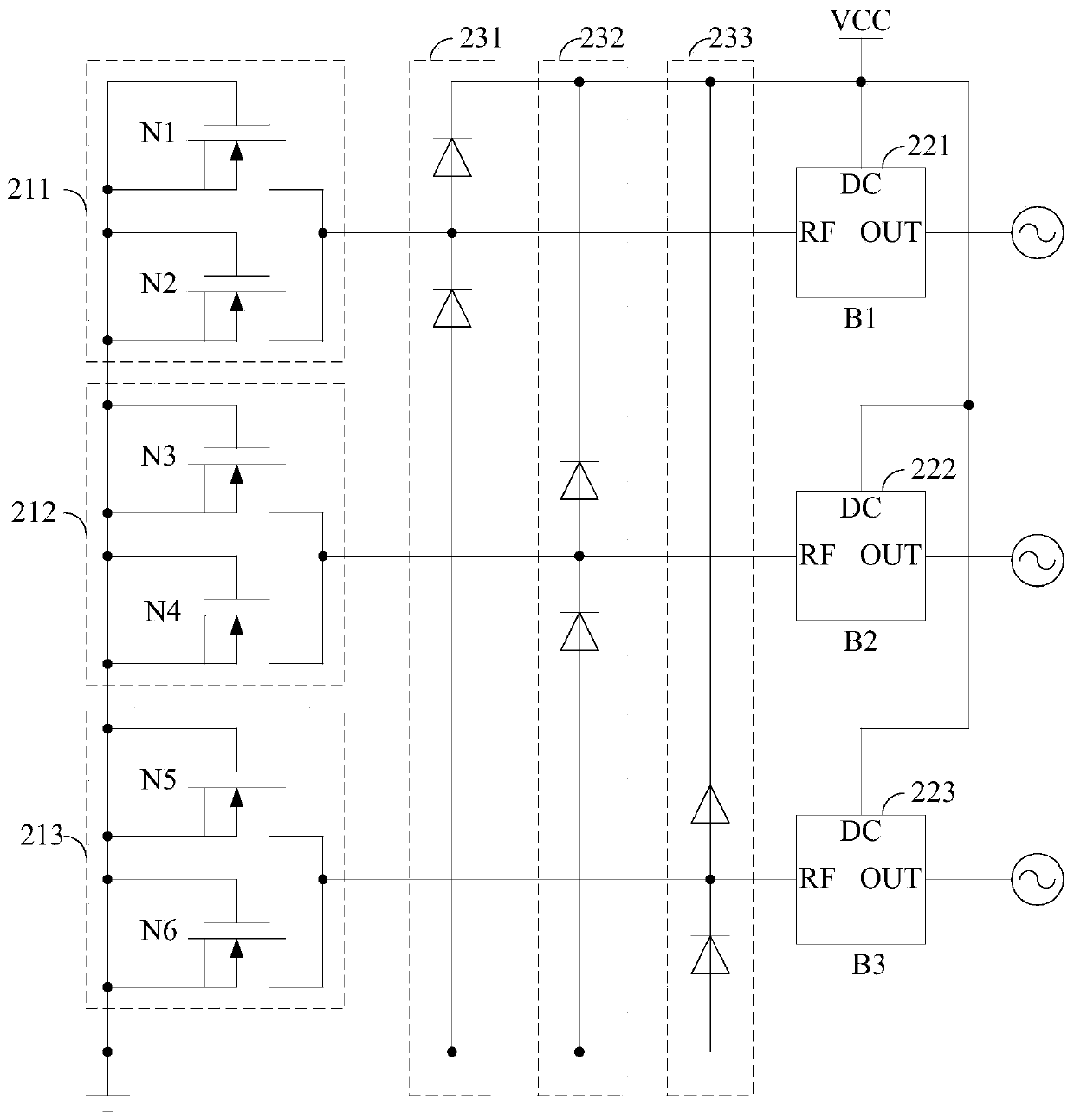
[0042] figure 2 It is a circuit diagram of a single high-energy particle ionization charge test circuit in this embodiment, and the single high-energy particle ionization charge test circuit includes three high-energy particle capture modules and three signal detection modules. The three high-energy particle capture modules are: the first high-energy particle capture module 211, the second high-energy particle capture module 212 and the third high-energy particle capture module 213; the three signal detection modules are: the first signal detection module 221, The second signal detection module 222 and the third signal detection module 223, the first signal detection module 221 corresponds to the first high-energy particle capture module 211, the second signal detection module 222 corresponds to the second high-energy particle capture Module 212 corresponds, and the third signal detection module 223 corresponds to the third high-energy particle capture module 213 .

[0043] ...

Embodiment 2

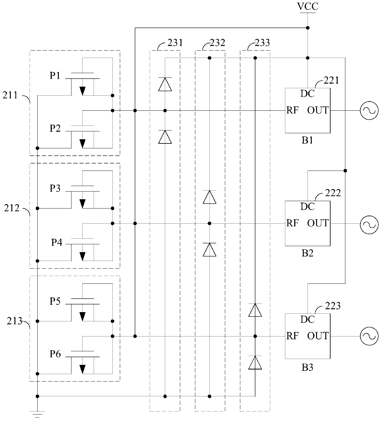
[0050] image 3 It is the circuit diagram of the single high-energy particle ionization charge test circuit of the present embodiment, and figure 2Compared with the corresponding embodiment, the difference is that: the first high-energy particle capture module 211 includes a first PMOS transistor P1 and a second PMOS transistor P2, the gate of the first PMOS transistor P1, the gate of the first PMOS transistor P1 The source of the second PMOS transistor P2, the gate of the second PMOS transistor P2, and the source of the second PMOS transistor P2 are connected to the power supply terminal VCC and serve as the output terminal of the first high-energy particle capture module 211, and the first The drain of the PMOS transistor P1 and the drain of the second PMOS transistor P2 are grounded; the second high-energy particle capture module 212 includes a third PMOS transistor P3 and a fourth PMOS transistor P4, and the gate of the third PMOS transistor P3 pole, the source of the th...


PUM


Abstract

The invention discloses a single high-energy particle ionization charge test circuit, which comprises M high-energy particle capture modules and M signal detection modules, the M high-energy particlecapture modules and the M signal detection modules are in one-to-one correspondence, and M is a positive integer not less than 2; each high-energy particle capture module comprises N field effect transistors connected in parallel, the field effect transistors are used for capturing high-energy particles and generating transient current signals flowing through the field effect transistors when thehigh-energy particles are captured, and N is a positive integer; and the signal detection modules are used for detecting the transient current signals generated by the corresponding high-energy particle capture modules and outputting test signals when the transient current signals are detected. According to the single high-energy particle ionization charge test circuit provided by the invention, the high-energy particle ionization charge cloud radius and the influence range can be tested, theoretical guidance is provided for the layout topological structure design of an anti-radiation reinforced integrated circuit, and the anti-radiation capability of the integrated circuit is improved.

Description

technical field [0001] The invention relates to the technical field of integrated circuits, in particular to a single high-energy particle ionization charge test circuit. Background technique [0002] The single event effect is a phenomenon in which a single high-energy particle in the space radiation environment generates and accumulates effective ionized charges through direct or indirect ionization in the device material, and is collected by the sensitive node of the device, resulting in a change in the working state of the device or failure of the function. When a single event effect occurs in a device in a memory, a latch, or a register, the logic state of a circuit unit changes, that is, a single event upset occurs. [0003] Multi-bit flipping refers to the situation where a single particle incident on the device causes flipping of multiple memory cells corresponding to the physical address. With the development of semiconductor manufacturing technology, the size of d...

Claims


Application Information

Patent Timeline
Patent Type & Authority Applications(China)
IPC IPC(8): G01R31/28
Inventor 闫薇薇曾传滨高林春李晓静倪涛李多力罗家俊韩郑生
Owner INST OF MICROELECTRONICS CHINESE ACAD OF SCI
Why Eureka
Try Eureka