Miniaturized and compact duplexer based on thin film integrated passive device technology

An integrated passive device, compact technology, applied in waveguide-type devices, electrical components, circuits, etc., can solve the problems of large size and unstable performance of duplexers, and achieve improved performance, high quality factor, and high precision. Effect

Active Publication Date: 2021-07-13
HARBIN INST OF TECH
View PDF5 Cites 0 Cited by
  • Summary
  • Abstract
  • Description
  • Claims
  • Application Information

AI Technical Summary

Problems solved by technology

[0003] The purpose of the present invention is to provide a miniaturized and compact duplexer based on thin-film integrated passive device technology in order to solve the problems of large size and unstable performance in the working process of the existing planar cascaded duplexer

Method used


Image

  • Miniaturized and compact duplexer based on thin film integrated passive device technology
  • Miniaturized and compact duplexer based on thin film integrated passive device technology
  • Miniaturized and compact duplexer based on thin film integrated passive device technology

Examples


specific Embodiment approach 1

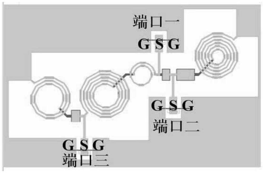
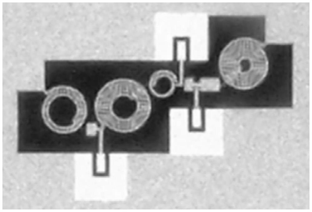
[0021] Embodiment 1: The miniaturized and compact duplexer based on thin-film integrated passive device technology in this embodiment includes a high-pass filter and a low-pass filter, the high-pass filter is coupled to signal port one P1 and signal port two P2, and the low-pass filter The filter is coupled to the signal port one P1 and the signal port three P3, where the high-pass filter is composed of the second capacitor C 2 Parallel first capacitance inductance resonant circuit (loop) is formed, and described first capacitance inductance resonant circuit is made of No. 1 capacitance C 1 and the No. 1 inductor L 1 series; wherein the low-pass filter is made up of two series inductors connected in parallel with the second capacitor-inductance resonant circuit (loop), and the two series inductors are composed of the second inductor L 2 and No. 4 inductance L 4 series, the second capacitor inductance resonant circuit consists of the third capacitor C 3 and No. 3 inductance ...

specific Embodiment approach 2

[0024] Specific embodiment two: the difference between this embodiment and specific embodiment one is that the inductance element in the high-pass filter and the low-pass filter is a spiral inductor, and the capacitive element in the high-pass filter and the low-pass filter is a MIM (metal-medium - metal) type capacitors.

specific Embodiment approach 3

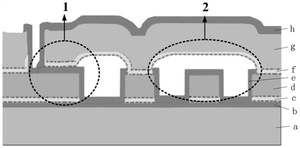
[0025] Specific Embodiment Three: In this embodiment, the preparation method of a miniaturized and compact duplexer based on thin film integrated passive device technology is implemented according to the following steps:

[0026] 1. Cleaning and polishing the surface of the substrate a to obtain a clean substrate;

[0027] 2. Depositing the first SiNx layer b on the clean substrate by plasma-enhanced chemical vapor deposition;

[0028] 3. Sputtering and depositing the first seed metal layer c on the surface of the first SiNx layer b, and then covering the wafer with a photomask, using photoresist to form a pattern of the bottom metal according to the circuit structure of a broadband miniaturized and compact duplexer, The bottom metal layer d is formed by an electroplating process, and the bottom metal layer d is used as the bottom metal of the MIM capacitor and the spiral metal of the spiral inductor, and the photoresist is removed after electroplating and the first seed metal...


PUM

PropertyMeasurementUnit
thicknessaaaaaaaaaa
thicknessaaaaaaaaaa
thicknessaaaaaaaaaa

Abstract

A miniaturized and compact duplexer based on thin-film integrated passive device technology, the invention belongs to the field of microwave devices, and in particular relates to a miniaturized duplexer, which solves the problem that the size of the existing planar cascaded duplexer is relatively large. The problem of performance instability during the work process. The compact duplexer of the present invention includes a high-pass filter and a low-pass filter, the high-pass filter is coupled to signal port one and signal port two, and the low-pass filter is coupled to signal port one and signal port three, wherein the high-pass filter consists of two No. capacitor in parallel with the first capacitor-inductance resonant circuit, and the low-pass filter is composed of two serial inductors in parallel with the second capacitor-inductor resonant circuit; the miniaturized and compact duplexer is made into a multi-layer structure through thin film integrated passive device technology. The size of the compact duplexer of the present invention is only 1.9mm×0.8mm, and the thickness is 0.2mm, and the manufacturing process of the present invention has high precision and stable device performance.

Description

technical field [0001] The invention belongs to the field of microwave devices, in particular to a miniaturized duplexer. Background technique [0002] GaAs substrate-based passive device processing technology has become one of the most promising technologies for the development of next-generation wireless communication systems. The processing methods commonly used in the traditional economy are printed circuit board technology (PCB), low temperature co-fired ceramic (LTCC) technology and complementary metal oxide semiconductor (CMOS) technology. The line width and limited spacing resolution of PCB technology will further limit the miniaturization and dimensional accuracy of RF devices; the mismatching speed of ceramic sintering and densification in LTCC technology will lead to uneven distribution on the surface of the substrate and reduce the adhesion of metal wires; Highly integrated CMOS technology can realize passive, active and digital functions in one module, but its ...

Claims


Application Information

Patent Timeline
Patent Type & Authority Patents(China)
IPC IPC(8): H01P5/16H01P11/00
CPCH01P5/16H01P11/00
Inventor 王琮于赫
Owner HARBIN INST OF TECH
Why Eureka
Try Eureka