Perovskite solar cell device and method for manufacturing same

A solar cell and perovskite technology, applied in the direction of final product manufacturing, sustainable manufacturing/processing, circuits, etc., can solve the problems of limited commercial applications, high production costs, low mobility, etc., and achieve high energy conversion efficiency.

Pending Publication Date: 2019-08-09
UNIV OF ELECTRONICS SCI & TECH OF CHINA
View PDF8 Cites 9 Cited by
  • Summary
  • Abstract
  • Description
  • Claims
  • Application Information

AI Technical Summary

Problems solved by technology

The n-type electron transport material used in the planar structure is generally a metal oxide semiconductor material, and the p-type hole transport material is generally an organic hole transport material, and the organic hole transport material used is often required due to its low mobility. High energy conversion efficiency can only be obtained by doping other material devices, which limits its further commercial application
However, the n-type electron transport materials used in the planar inversion structure are generally fullerene and its derivatives. Such materials have the disadvantages of high production cost and difficult purification, which restrict their large-scale production.

Method used


Image

  • Perovskite solar cell device and method for manufacturing same
  • Perovskite solar cell device and method for manufacturing same
  • Perovskite solar cell device and method for manufacturing same

Examples


example 1

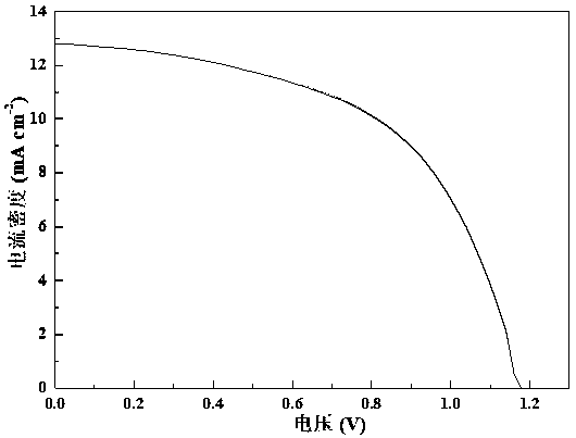
[0065] Take several ITO conductive glass substrates with the same batch number, the thickness of ITO is about 200 nanometers, and its square resistance is about 20 ohms / square. Sequentially use micron semiconductor special detergent, deionized water, acetone, and isopropanol to ultrasonically clean for 15 minutes to remove dirt on the substrate surface. Then put it into an incubator to dry at 80 degrees Celsius. Subsequently, inorganic nickel oxide (NiO x ) as the hole transport layer, by adjusting the thickness of the inorganic hole transport layer to 20-50 nanometers and then optimizing the energy conversion efficiency of the all-inorganic perovskite battery device, the evaporated nickel oxide substrate is transferred to the anhydrous In an oxygen-free glove box filled with high-purity nitrogen. In this glove box, the component prepared by spin coating is CsPbI 2 The hybrid inorganic perovskite photoactive layer of Br was then heated using a two-step heating method, first...

example 2

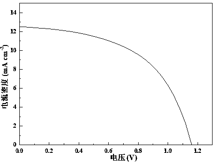
[0071] The preparation process is the same as that in Example 1. A number of ITO conductive glass substrates with the same batch number are taken. The thickness of the ITO is about 200 nanometers, and its sheet resistance is about 20 ohms / square. Sequentially use micron semiconductor special detergent, deionized water, acetone, and isopropanol to ultrasonically clean for 15 minutes to remove dirt on the substrate surface. Then put it into an incubator to dry at 80 degrees Celsius. Subsequently, inorganic nickel oxide (NiO x ) as the hole transport layer, the evaporated nickel oxide substrate was annealed in the air at 200 degrees Celsius for 1 hour, and then transferred to a glove box filled with high-purity nitrogen gas without water and oxygen. In this glove box, the component prepared by spin coating is CsPbI 2 The hybrid inorganic perovskite photoactive layer of Br was then heated using a two-step heating method, first on a heating stage at 40 °C for 4 min, then at 160 °...

example 3

[0075] The preparation process is the same as that in Example 1. A number of ITO conductive glass substrates with the same batch number are taken. The thickness of the ITO is about 200 nanometers, and its sheet resistance is about 20 ohms / square. Sequentially use micron semiconductor special detergent, deionized water, acetone, and isopropanol to ultrasonically clean for 15 minutes to remove dirt on the substrate surface. Then put it into an incubator to dry at 80 degrees Celsius. Subsequently, inorganic nickel oxide (NiO x ) as the hole transport layer, the evaporated nickel oxide substrate was annealed in the air at 300 degrees Celsius for 1 hour, and then transferred to a glove box filled with high-purity nitrogen gas without water and oxygen. In this glove box, the component prepared by spin coating is CsPbI 2 The hybrid inorganic perovskite photoactive layer of Br was then heated using a two-step heating method, first on a heating stage at 40 °C for 4 min, then at 160 °...


PUM


Abstract

The embodiment of the invention discloses a perovskite solar cell device and a method for manufacturing the same. The perovskite solar cell device comprises a substrate, an anode (ITO), an electron beam evaporation inorganic hole transport layer (NiOx), an inorganic perovskite light absorbing layer, an electron beam evaporation inorganic electron transport layer (Nb2O5), and an electron beam evaporation cathode (Ag) which are successively stacked. The all-inorganic perovskite solar cell device and the manufacturing method thereof obtain high energy conversion efficiency, and the hole transportlayer nickel oxide can achieve doping of different elements and different concentrations by double-source electron beam co-evaporation so as to improve optical and electrical properties. The all-inorganic perovskite cell device has a low processing cost and can achieve large-area processing, and has a good application prospect in the field of solar cells.

Description

technical field [0001] The invention relates to the technical field of electronic materials, in particular to a perovskite solar cell and a manufacturing method thereof. Background technique [0002] As early as 2006, the research group of Professor Miyasaka of Toin Yokohama University in Japan tried to use perovskite materials as light-absorbing materials in dye-sensitized solar cells. In 2009, they first reported dyes with a solar energy conversion efficiency of 3-4%. Sensitized perovskite solar cells (J.Am.Chem.Soc., 2009, 131, 6050). Then Professor Nam-Gyu Park's research group at Sungkyunkwan University in South Korea optimized the concentration of the precursor solution and the annealing temperature, which nearly doubled the energy conversion efficiency (Nanoscale, 2011, 3, 4088), and the perovskite solar cell is truly It has attracted attention that they used perovskite materials in an all-solid-state structure similar to organic thin-film solar cells, and greatly im...

Claims


Application Information

Patent Timeline
Patent Type & Authority Applications(China)
IPC IPC(8): H01L31/18H01L31/072
CPCH01L31/18H01L31/072Y02E10/50Y02P70/50
Inventor 刘欣李严波
Owner UNIV OF ELECTRONICS SCI & TECH OF CHINA
Why Eureka
Try Eureka