Single ZnO:Ga micron wire heterojunction base point light source device and preparation method thereof

A micro-wire and heterojunction technology, applied in semiconductor devices, electrical components, nanotechnology, etc., can solve the problems of low luminous efficiency, difficult p-type doping, low effective carrier injection rate, etc., to suppress surface defects. , the effect of improving the local conductivity and increasing the effective injection rate

Inactive Publication Date: 2019-08-16
NANJING UNIV OF AERONAUTICS & ASTRONAUTICS
View PDF3 Cites 14 Cited by
  • Summary
  • Abstract
  • Description
  • Claims
  • Application Information

AI Technical Summary

Problems solved by technology

However, due to the existence of a large number of zinc interstitial and oxygen vacancy defects in ZnO materials, p-type doping is extremely d

Method used


Image

  • Single ZnO:Ga micron wire heterojunction base point light source device and preparation method thereof
  • Single ZnO:Ga micron wire heterojunction base point light source device and preparation method thereof
  • Single ZnO:Ga micron wire heterojunction base point light source device and preparation method thereof

Examples


Embodiment 1

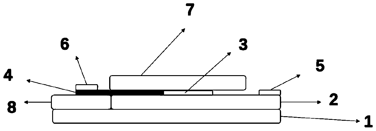
[0036] The first step: place the p-GaN substrate in a high-temperature tube furnace for annealing at 700-900°C for 1-2 hours, and then clean the p-GaN substrate with trichlorethylene, acetone, ethanol, and deionized water in sequence after annealing , dry with nitrogen, and finally use electron beam evaporation to evaporate two layers of electrodes on one end of p-GaN to form a 30nm thick Ni / Au electrode, and test the ohmic characteristics of the electrode.

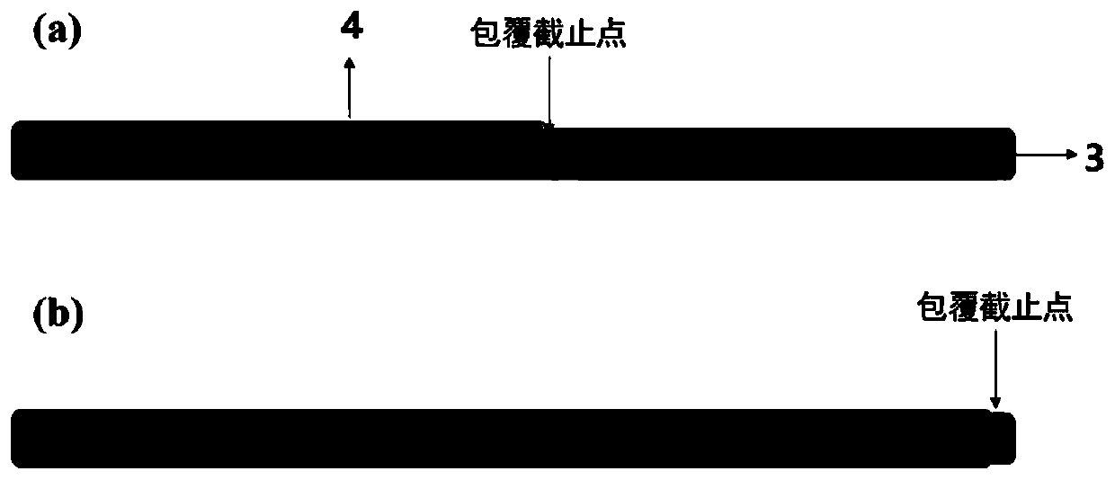
[0037] Step 2: Take a single quadrilateral ZnO:Ga micron wire with a length of 0.5cm to 1cm, and use a plasma sputtering device to sputter a layer of dense Ag nanoparticles with a thickness of 30nm on the surface of the ZnO:Ga micron wire. Among them, the mask plate used before sputtering is made of metal with different specifications, which is beneficial to shield sputtering in any area on the surface of the micron line; the sputtering target is an Ag target, the size is 50.8*1.0mm, the purity is 99.99%, and the working g...

Embodiment 2

[0041] The first step: place the p-GaN substrate in a high-temperature tube furnace for annealing at 700-900°C for 1-2 hours, and then clean the p-GaN substrate with trichlorethylene, acetone, ethanol, and deionized water in sequence after annealing , dry with nitrogen, and finally use electron beam evaporation to evaporate two layers of electrodes on one end of p-GaN to form a 30nm thick Ni / Au electrode, and test the ohmic characteristics of the electrode.

[0042] Step 2: Take a single quadrilateral ZnO:Ga micron wire with a length of 0.5cm to 1cm, and use a plasma sputtering device to sputter a layer of dense Ag nanoparticles with a thickness of 30nm on the surface of the ZnO:Ga micron wire. Among them, the mask plate used before sputtering is made of metal with different specifications, which is beneficial to shield sputtering in any area on the surface of the micron line; the sputtering target is an Ag target, the size is 50.8*1.0mm, the purity is 99.99%, and the working g...

Embodiment 3

[0046] The first step: place the p-GaN substrate in a high-temperature tube furnace for annealing at 700-900°C for 1-2 hours, and then clean the p-GaN substrate with trichlorethylene, acetone, ethanol, and deionized water in sequence after annealing , dry with nitrogen, and finally use electron beam evaporation to evaporate two layers of electrodes on one end of p-GaN to form a 30nm thick Ni / Au electrode, and test the ohmic characteristics of the electrode.

[0047] Step 2: Take a hexagonal ZnO:Ga single micron wire with a length of 0.8cm to 1.5cm, press the indium grain on one end, place the pressed indium grain end at the clamp of the self-made spin coater, and set the spin coating time to 20min , the pulling speed is 0.05mm / min, the concentration of the Ag nanowire solution used is about 0.03-0.2g / mL, the length of the Ag nanowire is 3-100um, and the width is 30-130nm, and then placed in a drying oven at 80°C for 10min.

[0048] Step 3: Transfer the micron wires obtained in...


PUM

PropertyMeasurementUnit
Thicknessaaaaaaaaaa
Electron mobilityaaaaaaaaaa
Lengthaaaaaaaaaa

Abstract

The invention discloses a single ZnO:Ga micron wire heterojunction base point light source device and a preparation method thereof, and belongs to the technical field of semiconductor optoelectronic devices. The device comprises a quartz base, a p-GaN substrate, and an AgNPs@ZnO:Ga composite system disposed above the p-GaN substrate, wherein the AgNPs@ZnO:Ga composite system includes a ZnO: Ga single micron wire, and an Ag nano particle layer which is controllably disposed on the surface of the ZnO: Ga single micron wire to form an Ag-coated ZnO:Ga micron wire composite structure. Sputtering or spin-coating the surface of the micron wire with chemically synthesized Ag nanoparticles can suppress the surface defects of ZnO and increase the effective injection rate of micron wire carriers. Further, the surface plasmons of Ag nanoparticles have extremely strong field limit and field enhancement characteristics, can limit the energy to a point, and regulate the carrier recombination area tothe same area to construct a low-dimensional point LED.

Description

technical field [0001] The invention relates to the technical field of semiconductor optoelectronic devices, and to a light-emitting diode, in particular to the production of a single ZnO:Ga micron wire heterojunction-based point light source. Background technique [0002] As a direct bandgap and wide bandgap semiconductor material of the II-VI group, ZnO has a bandgap of about 3.37eV and an exciton binding energy of up to 60meV at room temperature, and is widely used in light-emitting diodes and detectors in the ultraviolet band. In addition, the micro-nano structure of ZnO has excellent single crystal, natural optical cavity, controllable structure and morphology, and is expected to realize high-efficiency luminescence and low-threshold laser devices. However, due to the large number of zinc interstitial and oxygen vacancy defects in ZnO materials, p-type doping is extremely difficult, and the effective injection rate of carriers is low, which makes the luminous efficiency...

Claims


Application Information

Patent Timeline
IPC IPC(8): H01L33/00H01L33/26H01L33/14B82Y30/00B82Y40/00
CPCB82Y30/00B82Y40/00H01L33/002H01L33/005H01L33/14H01L33/26
Inventor 阚彩侠周祥博姜明明施大宁
Owner NANJING UNIV OF AERONAUTICS & ASTRONAUTICS
Why Eureka
Try Eureka