A repair preparation method of a trace amount of sn-doped perovskite film and all-inorganic perovskite solar cell

A perovskite and inorganic calcium technology, applied in the manufacture of circuits, electrical components, final products, etc., can solve the problems of perovskite film quality, limitations, and affecting the extraction efficiency of interface charges

Active Publication Date: 2022-02-08
深圳市运通天下科技有限公司
View PDF0 Cites 0 Cited by
  • Summary
  • Abstract
  • Description
  • Claims
  • Application Information

AI Technical Summary

Problems solved by technology

Unfortunately, CsPbBr produced by traditional one-step or two-step 3 The quality of perovskite film is worrying
Furthermore, CsPbBr with a conduction band (CB) of -3.3eV and a valence band (VB) of -5.6eV 3 The wide bandgap energy level of perovskite material 2.3eV limits its charge transport ability, and TiO 2 / CsPbBr 3 and CsPbBr 3 The existence of a high-energy barrier between the / Carbon interface seriously affects the extraction efficiency of interfacial charges. Based on these problems, it usually leads to the CsPbBr 3 Perovskite solar cells have an efficiency (PCE) of less than 10%

Method used


Image

  • A repair preparation method of a trace amount of sn-doped perovskite film and all-inorganic perovskite solar cell
  • A repair preparation method of a trace amount of sn-doped perovskite film and all-inorganic perovskite solar cell
  • A repair preparation method of a trace amount of sn-doped perovskite film and all-inorganic perovskite solar cell

Examples


Embodiment 1

[0035] This embodiment is an all-inorganic perovskite solar cell, which sequentially includes a layered conductive glass layer, an electron transport layer, an all-inorganic perovskite layer and a carbon electrode layer.

[0036] Use the sol-gel method to coat a layer of dense titanium dioxide film on the conductive glass as an electron transport layer. After heat treatment at 400-450°C, perform titanium tetrachloride hydrolysis reaction treatment on the dense titanium dioxide film, and place it in a box-type resistance furnace after drying. Sintering at 450-500°C for later use.

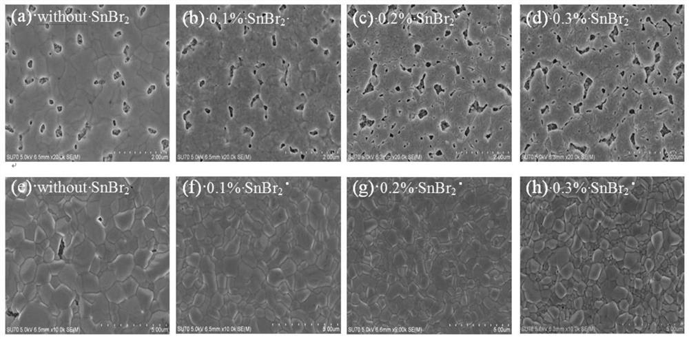
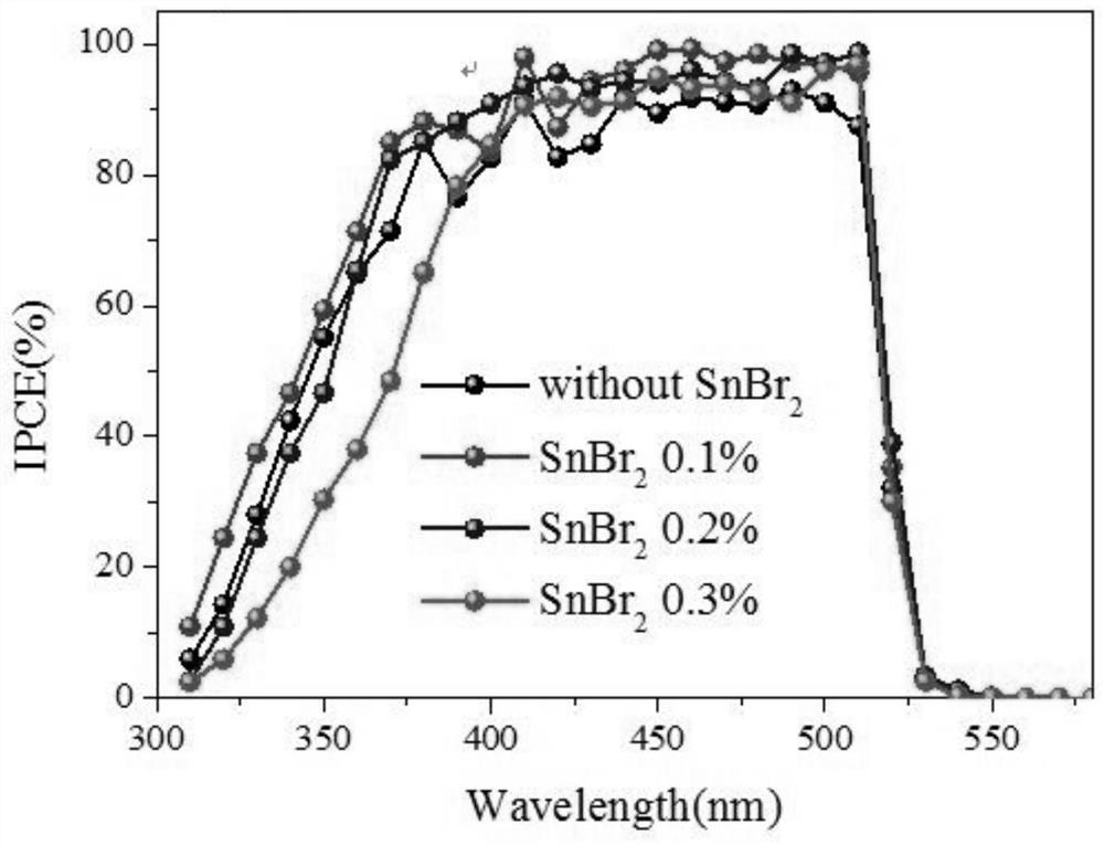
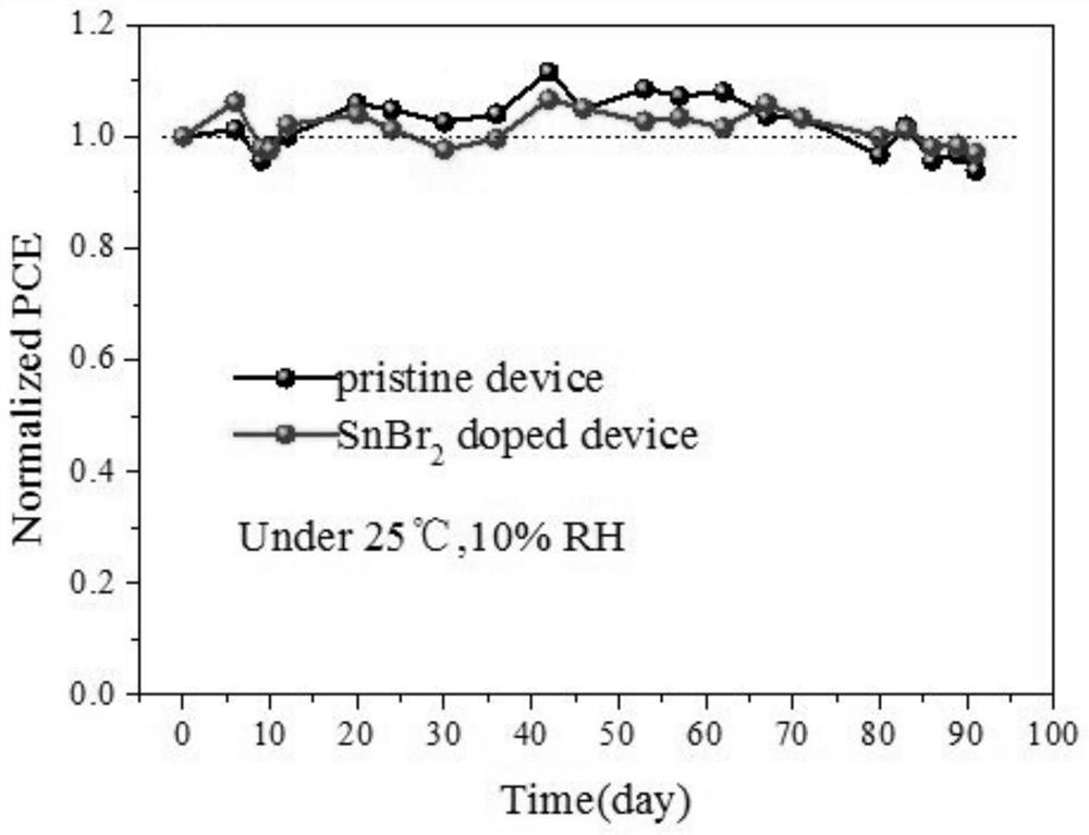
[0037] Dissolve lead bromide and tin bromide in DMF solution to form base solution, the molar concentration of lead bromide is 1mol / L, and the molar concentration of tin bromide is 0.001mol / L. Cesium bromide was dissolved in DMSO to form a modification solution, and the molar concentration of cesium bromide was 1mol / L. The substrate solution was spin-coated onto the electron transport layer to form ...

Embodiment 2

[0041]This embodiment is an all-inorganic perovskite solar cell, which sequentially includes a layered conductive glass layer, an electron transport layer, an all-inorganic perovskite layer and a carbon electrode layer.

[0042] Use the sol-gel method to coat a layer of dense titanium dioxide film on the conductive glass as an electron transport layer. After heat treatment at 400-450°C, perform titanium tetrachloride hydrolysis reaction treatment on the dense titanium dioxide film, and place it in a box-type resistance furnace after drying. Sintering at 450-500°C for later use.

[0043] Dissolve lead bromide and tin bromide in the DMF solution to form a base solution, the molar concentration of lead bromide is 1mol / L, and the molar concentration of tin bromide is 0.002mol / L. Cesium bromide was dissolved in DMSO to form a modification solution, and the molar concentration of cesium bromide was 1mol / L. The substrate solution was spin-coated onto the electron transport layer to ...

Embodiment 3

[0047] This embodiment is an all-inorganic perovskite solar cell, which sequentially includes a layered conductive glass layer, an electron transport layer, an all-inorganic perovskite layer and a carbon electrode layer.

[0048] Use the sol-gel method to coat a layer of dense titanium dioxide film on the conductive glass as an electron transport layer. After heat treatment at 400-450°C, perform titanium tetrachloride hydrolysis reaction treatment on the dense titanium dioxide film, and place it in a box-type resistance furnace after drying. Sintering at 450-500°C for later use.

[0049] Dissolve lead bromide and tin bromide in DMF solution to form base solution, the molar concentration of lead bromide is 1mol / L, and the molar concentration of tin bromide is 0.003mol / L. Cesium bromide was dissolved in DMSO to form a modification solution, and the molar concentration of cesium bromide was 1mol / L. The substrate solution was spin-coated onto the electron transport layer to form ...


PUM


Abstract

The invention discloses a preparation method for repairing a trace Sn-doped perovskite film and an all-inorganic perovskite solar cell, comprising the following steps: dissolving tin halide and lead halide into a DMF solution to form a base solution; dissolving the base solution Spin coating onto the surface of the substrate, and dry the base solution on the surface of the substrate to form a base layer on the surface of the substrate; dissolve cesium halide into DMSO to form a modification solution, spin the modification solution on the base layer for several times, and each time After the second spin coating is completed, heating, the modification solution and the base layer gradually react to form an all-inorganic perovskite layer. Tin halide destroys the film formed by the original lead halide, making the base layer into a loose and porous structure, which is more conducive to the reaction between cesium halide and lead halide in the later stage, and increases the reaction area between cesium halide and lead halide. After the cesium halide reacts, the pores are gradually filled, and the obtained all-inorganic perovskite layer has fewer pinholes and exhibits better charge extraction and charge transport capabilities.

Description

【Technical field】 [0001] The invention relates to a preparation method for repairing a trace Sn-doped perovskite film and an all-inorganic perovskite solar cell, belonging to the field of perovskite preparation methods. 【Background technique】 [0002] Perovskite solar cells have received unprecedented attention since their discovery, and their efficiency has grown from 3.8% to 23.7% since 2009. However, the vast majority of perovskite solar cells suffer from poor environmental stability. Among them, with CsPbBr 3 The all-inorganic perovskite solar cell with the perovskite light-absorbing layer structure is the best among the known perovskite solar cells with both efficiency and stability. Under unencapsulated conditions, it can maintain more than 85% of its original efficiency in the atmosphere for more than three months. Because CsPbBr 3 Perovskite has excellent environmental stability, so it can be prepared in the atmospheric environment, which is an advantage that oth...

Claims


Application Information

Patent Timeline
Patent Type & Authority Patents(China)
IPC IPC(8): H01L31/18H01L31/032
CPCH01L31/18H01L31/0321Y02P70/50
Inventor 诸跃进郭海燕裴越
Owner 深圳市运通天下科技有限公司
Why Eureka
Try Eureka