

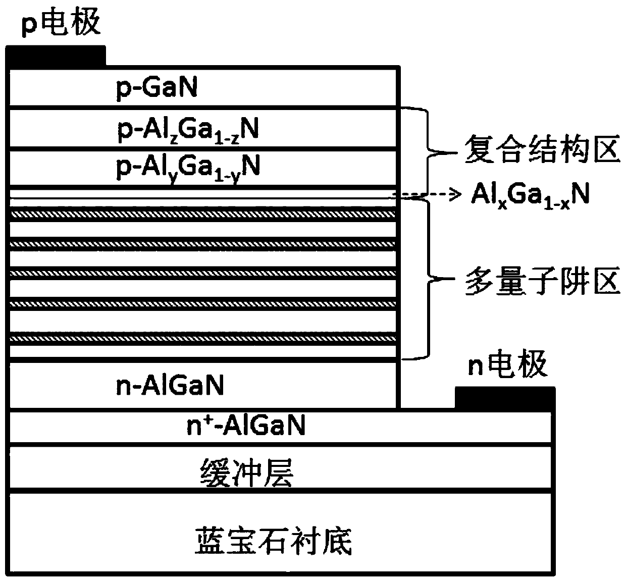
An ultraviolet led epitaxial structure
An epitaxial structure, ultraviolet technology, applied in the direction of semiconductor devices, electrical components, circuits, etc., can solve the problems of low internal quantum efficiency and light output power, achieve the effect of improving luminous performance, increasing light output power, and enhancing radiation recombination
- Summary
- Abstract
- Description
- Claims
- Application Information
AI Technical Summary
Problems solved by technology
Method used
Image

Examples
Embodiment 1
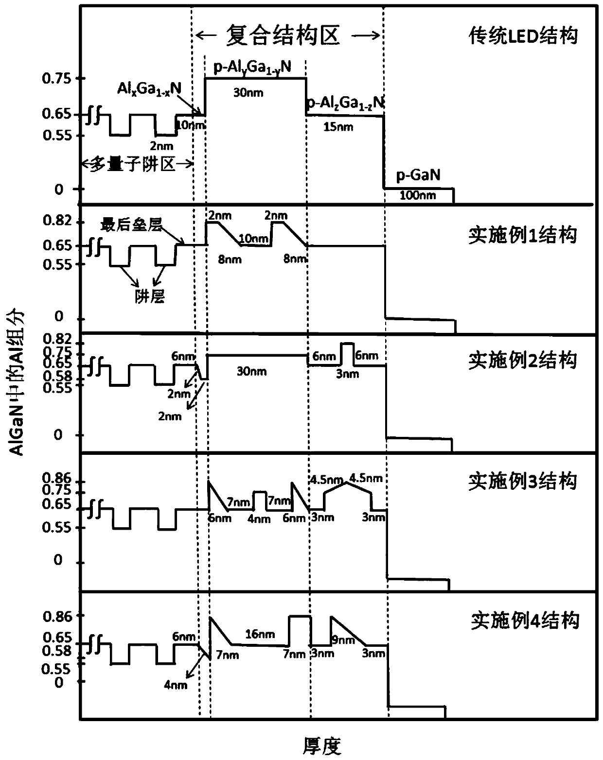
[0045] Different from the traditional structure, in this embodiment, the electron blocking layer in the composite structure region of the ultraviolet LED is designed as a double trapezoidal peak structure (similar to a double hump structure), while the electron blocking layer in the traditional structure is only a single Al component layer. attached figure 2 It is a schematic diagram of the change of Al composition in the compound structure region of different embodiments of the ultraviolet LED epitaxial structure of the present invention. For the structure of this example, see figure 2 The structural representation of embodiment 1 in. The double trapezoidal peak structure here uses a Mg-doped multi-Al component electron blocking layer, which in turn is 2nm thick p-Al 0.82 Ga 0.18 N, 8nm thick p-AlGaN graded layer (from Al 0.82 Ga 0.18 N linear gradient to Al 0.65 Ga 0.35 N), 10nm thick p-Al 0.65 Ga 0.35 N, 2nm thick p-Al 0.82 Ga 0.18 N and 8nm thick p-AlGaN graded...
Embodiment 2
[0048] This embodiment differs from the traditional structure in two points, in that the composite structure area adopts Al x Ga 1-x The N concave layer and a rectangular peak are added in the p-type hole injection layer. By regulating Al x Ga 1-x The Al component of the N material realizes the inverted trapezoidal peak structure of the concave layer, see the attached figure 2 The structure schematic diagram of embodiment 2 in. The inverted trapezoidal peak structure of the concave layer is composed of a 2nm thick AlGaN graded layer (by Al 0.65 Ga 0.35 N linear gradient to Al 0.58 Ga 0.42 N) and 2nm thick Al 0.58 Ga 0.42 N, while the hole injection layer is made of Mg doping concentration of 3 × 10 17 cm -3 6nm thick p-Al 0.65 Ga 0.35 N, 3nm thick p-Al 0.82 Ga 0.18 N and 6nm thick p-Al 0.65 Ga 0.35 N material composition, other structural layer parameters are the same as the traditional structure. The epitaxial structure growth technology and process conditi...
Embodiment 3
[0051] What this embodiment is different from the traditional structure is: three peaks are designed in the electronic blocking layer of the composite structure area, and for the combination of triangular peak, rectangular peak and triangular peak, a peak (by a rectangular peak) is set in the hole injection layer and a triangular peak), see attached figure 2 The structural representation of embodiment 3 in. The material structure of the electron blocking layer is that the Mg doping concentration is 3×10 17 cm -3 6nm thick graded layer (by Al 0.86 Ga 0.14 N linear gradient to Al 0.65 Ga 0.35 N), 7nm thick Al 0.65 Ga 0.35 N, 4nm thick Al 0.75 Ga 0.25 N, 7nm thick Al 0.65 Ga 0.35 N and 6nm thick graded layer (by Al 0.86 Ga 0.14 N linear gradient to Al 0.65 Ga 0.35 N). The hole injection layer is made of Mg doping concentration of 3 × 10 17 cm -3 3nm thick Al 0.65 Ga 0.35 N, 4.5nm thick gradient layer (by Al 0.75 Ga 0.25 N linear gradient to Al 0.86 Ga 0.1...
PUM
 Abstract
Description
Claims
Application Information