

Indium-doped N-type organic thin-film transistor and preparation method thereof
An organic thin film and transistor technology, which is applied in the field of indium-doped N-type organic thin-film transistor and its preparation, can solve the problems of limiting the development of flexible electronic devices and organic integrated circuits, high mobility, and shortage of N-type semiconductor materials, etc. Improved switching ratio and carrier mobility, low cost, and improved electrical performance
- Summary
- Abstract
- Description
- Claims
- Application Information
AI Technical Summary
Problems solved by technology
Method used
Image

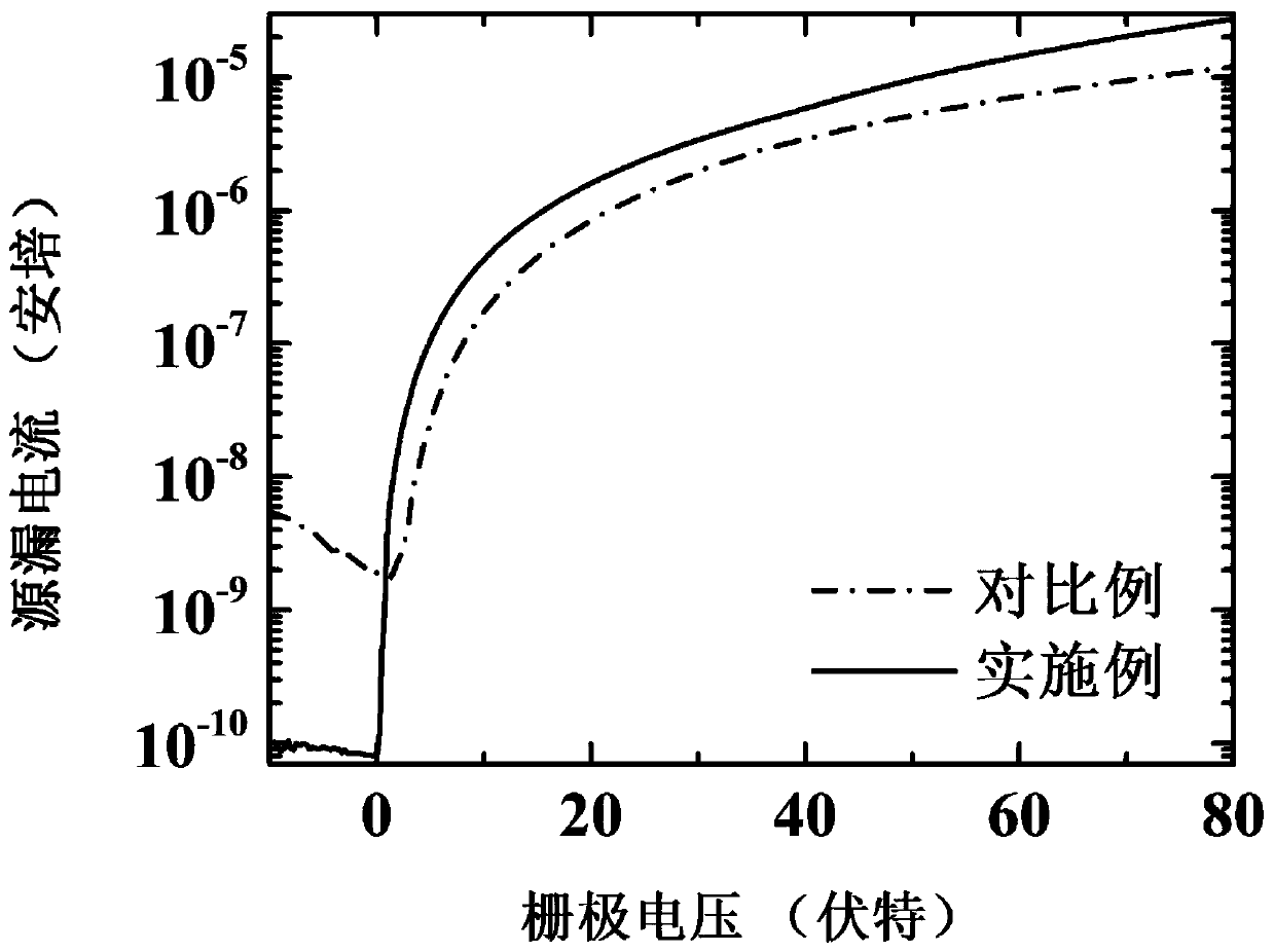
Examples
Embodiment
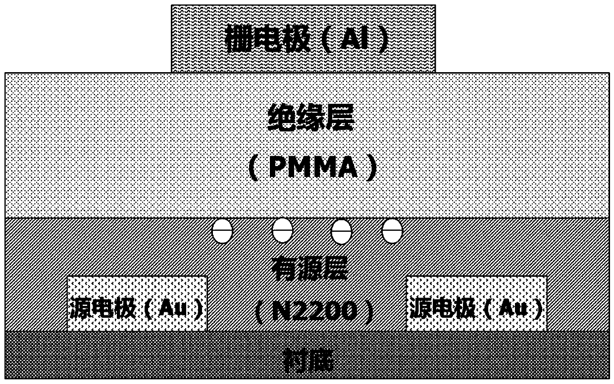
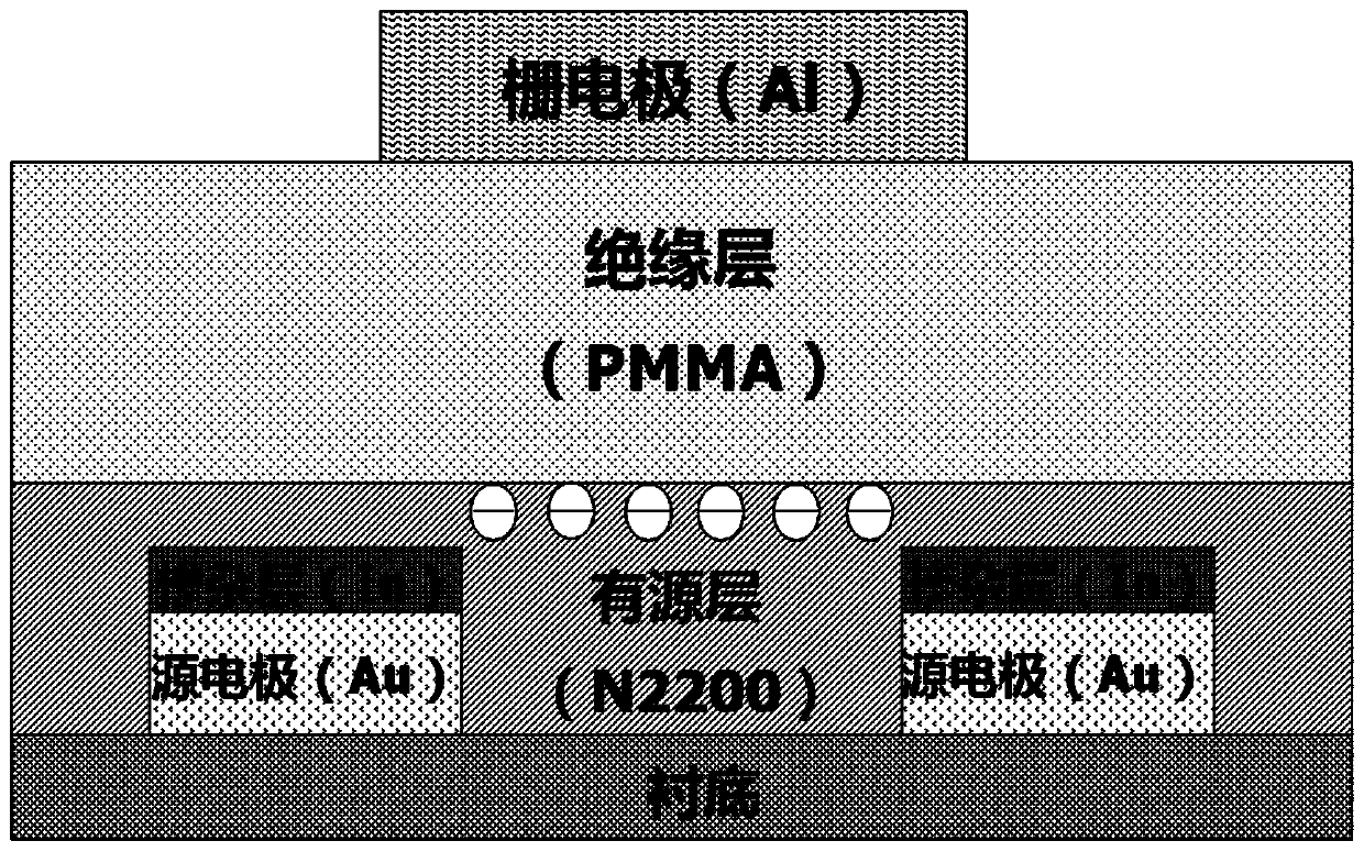
[0058] A1: Configuration of semiconductor solution
[0059] The N-type organic semiconductor material and the organic solvent are configured at a mass volume ratio of 8 mg / ml; wherein, the N-type organic semiconductor material is: [N,N'-bis(2-octyldodecyl)-1 , 4,5,8-naphthalene diimide-2,6-two bases-and-5,5'-(2,2'-bithiophene)] polymer (N2200); the organic solvent is chlorobenzene ;
[0060] A2: Configuration of insulating layer solution
[0061] The insulating layer material and the highly soluble organic solvent are configured with a mass volume ratio of 80mg / ml; wherein, the insulating layer material is polymethacrylate (PMMA); the highly soluble organic solvent is methyl acetate ester;
[0062] A3: Dissolution of the solution
[0063] Place the configured semiconductor solution and insulating layer solution on the heating plate at 60°C for 24 hours to dissolve;
[0064] Step 2: Preparation of Devices
[0065] B1: Cleaning of the substrate
[0066] Select an insulati...
PUM
| Property | Measurement | Unit |
|---|---|---|
| Thickness | aaaaa | aaaaa |
Abstract
Description
Claims
Application Information