Method for preparing three-dimensional metal micro-nano structure

A micro-nano structure and metal technology, applied in the manufacture of micro-structure devices, micro-structure technology, micro-structure devices, etc., can solve the problems of complex preparation process, achieve the effect of realizing broadband transmission, and the preparation process is simple and easy to operate

Inactive Publication Date: 2019-09-24
中山科立特光电科技有限公司
View PDF0 Cites 2 Cited by
  • Summary
  • Abstract
  • Description
  • Claims
  • Application Information

AI Technical Summary

Problems solved by technology

[0005] In order to solve the problems in the prior art that the preparation of three-dimensional metal micro-nano structures requires overlaying, multiple exposures, multiple coatings, and complicated preparation processes, the present invention provides a method for preparing three-dimensional metal micro-nano structures. A three-dimensional metal micro-nano structure can be prepared with one exposure and coating, and the preparation precision is high

Method used


Image

  • Method for preparing three-dimensional metal micro-nano structure
  • Method for preparing three-dimensional metal micro-nano structure
  • Method for preparing three-dimensional metal micro-nano structure

Examples


Embodiment 1

[0031] Step 1: Prepare the glass substrate 3, prepare the glass substrate 3 and clean it for use;

[0032] in particular:

[0033] The glass substrate 3 is specifically an ITO glass substrate. Prepare an ITO glass substrate 3 with a thickness of 1.0 mm and a length and width of 30.0 mm×30.0 mm, and put the prepared ITO glass into a washing solution for cleaning, and use deionized water to ultrasonically 5- After 10 minutes, use acetone to sonicate for 5-10 minutes, then use alcohol to sonicate for 5-10 minutes, and finally dry it with a nitrogen gun and put it in a nitrogen cabinet for later use.

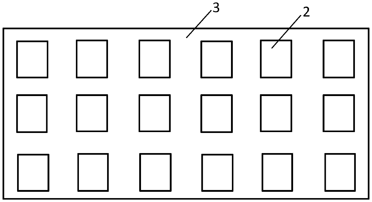
[0034] Step 2: Coating photoresist: throw two layers of positive photoresist on the surface of the glass substrate with a glue shaker; electron beam exposure structure pattern: design a square periodic array structure with a pattern generator; use an electron beam to design Fixed area exposure, the electron beam dose used is the first dose;

[0035] developing and fixing;

[0036...

Embodiment 2

[0051] For the three-dimensional metal micro-nano structure prepared in this example, only the thickness of the metal material layer 3 vertically evaporated by the electron beam evaporation coater is changed, and the preparation process is the same as that in Example 1.

[0052] in particular:

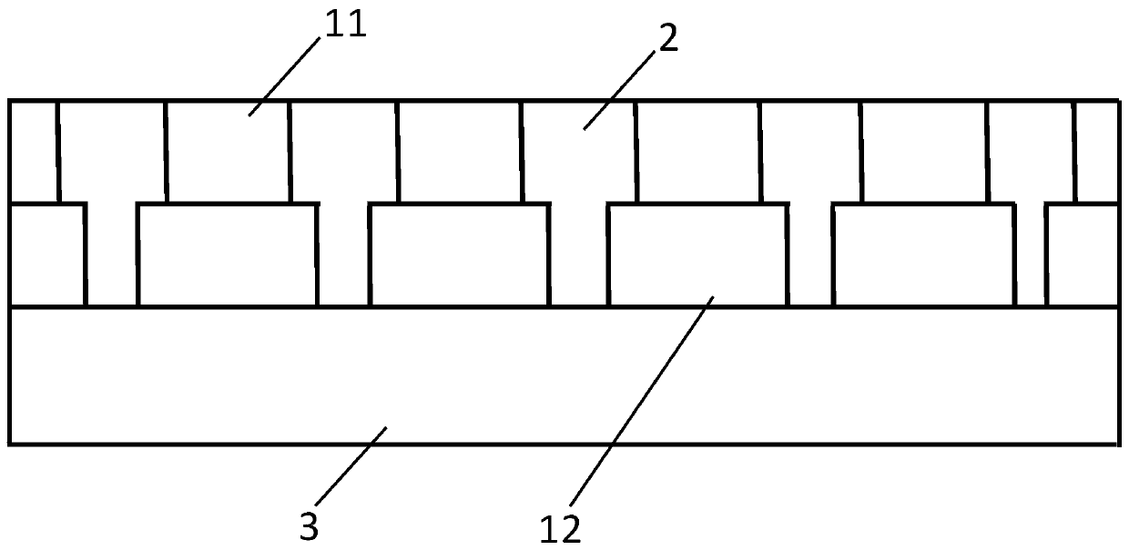
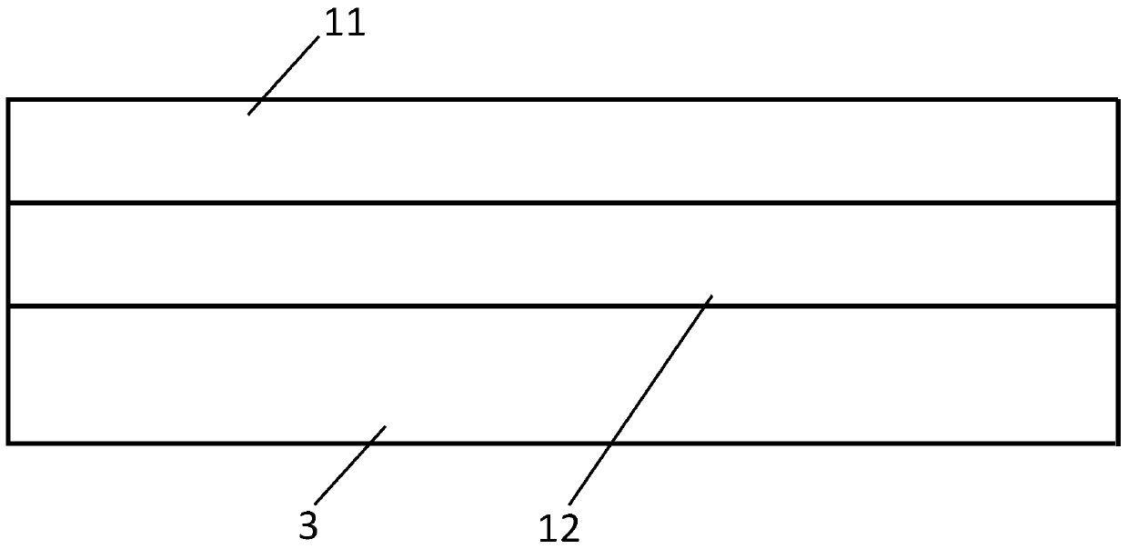
[0053] When coating the positive photoresist on the surface of the substrate with the glue spinner, the speed of the glue spinner is controlled, and then the thickness of the positive photoresist can be controlled, and the speed of the glue spinner is set at 1000rpm~6000rpm , and the time is set to 60s. The concrete step of described coating photoresist is, at first on the ITO glass substrate 3 spin-coating the positive resist with solid content of 4% with the glue-spinning machine, drying to form the first film 12, then spin-coating a layer with solid content of 2% positive resist is dried to form the second film 11 .

[0054] The three-dimensional metal micro-nano structure prepare...

Embodiment 3

[0056] For the three-dimensional metal micro-nano structure prepared in this example, only the angle of the metal material layer 3 evaporated by the electron beam evaporation coater is changed, and the preparation process is the same as that in Example 1.

[0057] in particular:

[0058] When adopting the electron beam vacuum evaporation coating instrument to vertically evaporate the metal material 3, by obliquely evaporating the metal material layer 3, the thickness of the metal material evaporated by the electron beam evaporation coating instrument is greater than the thickness of the first film 12, such as figure 1 shown. After evaporating the coating, the process of stripping the photoresist is carried out, soaking the ITO glass after evaporating the metal with acetone, dissolving the first film 12 and the second film 11, and the soaking time is at least 30 minutes. Afterwards, the substrate was blown dry with a nitrogen gun to obtain a three-dimensional chiral metal micro-...


PUM


Abstract

The invention relates to the field of micro-nano structure preparation, in particular to a method for preparing a three-dimensional metal micro-nano structure, which mainly comprises the steps of photoresist coating, electron beam exposure, developing and fixing, metal material evaporation and photoresist stripping. In the preparation process, the double-layer metal micro-nano structure can be prepared only by once exposure and once evaporation, and the parameters of the structure can be adjusted through the dosage of an electron beam. The preparation method is simple and convenient to operate, and the process of preparing the multi-layer structure by overlay is avoided.

Description

technical field [0001] The invention relates to the field of micro-nano structure preparation, in particular to a method for preparing a three-dimensional metal micro-nano structure. Background technique [0002] With the rapid development of nanoscience, nanomaterials and devices have been widely used in various fields of human life, such as electronics, biosensing, semiconductor chips, new optical materials, and biomedicine. However, any application of nanomaterials in these fields must rely on nanofabrication technology, that is, the technology of manipulating and processing materials in the nanoscale range. Therefore, the development of high-efficiency, high-resolution, and low-cost production of nanomaterials and devices has become a focus of nanotechnology. [0003] At present, in the research of nanoelectronics and nanodevices, there are mainly ultraviolet lithography, electron beam lithography (EBL), X-ray lithography (X-ray Lithograph), focused ion beam technology ...

Claims


Application Information

Patent Timeline
Patent Type & Authority Applications(China)
IPC IPC(8): B81C1/00G03F7/00B82Y40/00
CPCB81C1/00031B81C1/00373B81C1/00388B81C1/00531B82Y40/00G03F7/0035
Inventor 不公告发明人
Owner 中山科立特光电科技有限公司
Why Eureka
Try Eureka