Method for forming optical waveguide quantum chip on gradual periodically polarized lithium tantalate by proton exchange method

A technology of proton exchange and periodic polarization, applied in the direction of optical waveguide light guide, light guide, optics, etc., can solve the problems of complex processing steps, improper process control, waveguide scattering loss, etc., to improve process stability, easy large-scale production, and low cost low effect

Active Publication Date: 2019-09-27
SHANDONG UNIV
View PDF12 Cites 5 Cited by
  • Summary
  • Abstract
  • Description
  • Claims
  • Application Information

AI Technical Summary

Problems solved by technology

However, the loading method in this patent application must first form a planar thin film structure of materials such as lithium niobate and lithium tantalate, and then form a loaded waveguide on this basis, and the processing steps are complicated.
Furthermore, the loading ridge material is amorphous, and improper process control can easily cause large waveguide scattering loss

Method used


Image

  • Method for forming optical waveguide quantum chip on gradual periodically polarized lithium tantalate by proton exchange method
  • Method for forming optical waveguide quantum chip on gradual periodically polarized lithium tantalate by proton exchange method
  • Method for forming optical waveguide quantum chip on gradual periodically polarized lithium tantalate by proton exchange method

Examples


Embodiment 1

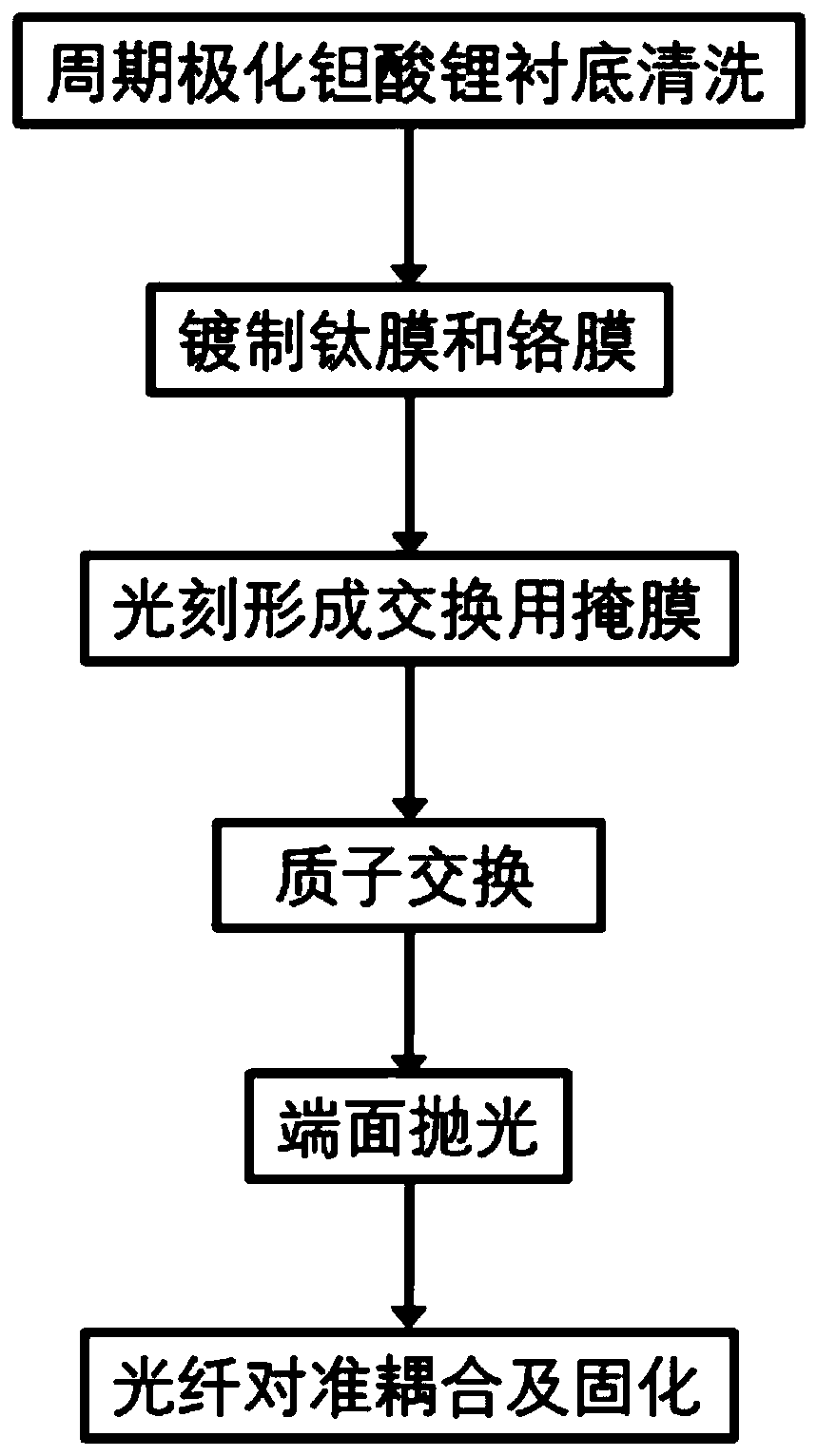
[0049] A method of forming an optical waveguide quantum chip on a graded periodic poled lithium tantalate by using a proton exchange method, such as figure 1 shown, including the following steps:

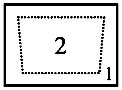
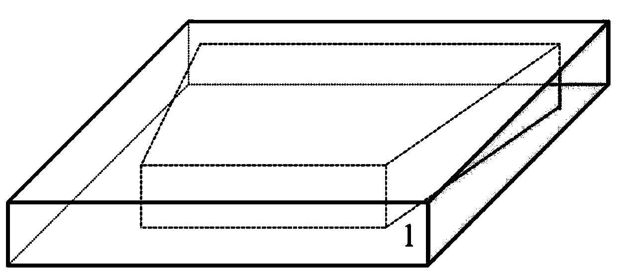
[0050] (1) Clean the magnesium-doped gradual periodic poled lithium tantalate (polarization period 18-22 microns) substrate 1 with a length of 2 cm and a width of 0.7 cm, and dry the sample with nitrogen gas. The substrate structure is as follows: Figure 2(a) , 2(b) As shown, wherein 2(a) is a top view, and Fig. 2(b) is a side view;

[0051] (2) Utilize an electron beam evaporation coating machine to plate a 15nm thick titanium film on the substrate surface;

[0052] (3) Utilize an electron beam evaporation coating machine to plate a 100nm thick chromium film on the substrate surface;

[0053] (4) Use a commercial ultraviolet exposure machine to photolithographically form a 9-micron-wide strip-shaped optical waveguide pattern on the surface of lithium tantalate, such as image ...

Embodiment 2

[0060] A method for forming an optical waveguide quantum chip on a graded periodic poled lithium tantalate by using a proton exchange method, comprising the following steps:

[0061] (1) Clean the magnesium-doped gradual periodic poled lithium tantalate (polarization period 7.5-8.2 microns) substrate with a length of 1.2 cm and a width of 0.7 cm, and dry the sample with nitrogen;

[0062] (2) Utilize an electron beam evaporation coating machine to plate a 10nm thick titanium film on the substrate surface;

[0063] (3) Utilize an electron beam evaporation coating machine to plate an 80nm thick chromium film on the substrate surface;

[0064] (4) Use a commercial ultraviolet exposure machine to photolithographically form a 6.6-micron-wide strip-shaped optical waveguide pattern on the surface of lithium tantalate, and corrode to form a mask sample for proton exchange;

[0065] (5) Exchange the mask sample in benzoic acid for 60 minutes at 200 degrees Celsius;

[0066] (6) Optic...

Embodiment 3

[0070] A method for forming an optical waveguide quantum chip on a graded periodic poled lithium tantalate by using a proton exchange method, comprising the following steps:

[0071] (1) Clean the magnesium-doped gradual periodic poled lithium tantalate (polarization period 8.8-9.7 microns) substrate with a length of 1.2 cm and a width of 0.7 cm, and dry the sample with nitrogen;

[0072] (2) Utilize an electron beam evaporation coating machine to plate a 10nm thick titanium film on the substrate surface;

[0073] (3) Utilize an electron beam evaporation coating machine to plate a 70nm thick chromium film on the substrate surface;

[0074] (4) Use a commercial ultraviolet exposure machine to photolithographically form a 5-micron-wide strip-shaped optical waveguide pattern on the surface of lithium tantalate, and corrode to form a mask sample for proton exchange;

[0075] (5) Exchange the mask sample in benzoic acid for 50 minutes at 200 degrees Celsius;

[0076] (6) Opticall...


PUM


Abstract

The invention relates to a method for forming an optical waveguide quantum chip on gradual periodically polarized lithium tantalate by a proton exchange method, and belongs to the field of optoelectronic device preparation methods. The method comprises the following steps: a gradual periodically polarized lithium tantalate is cleaned; a titanium film and a chromium film are sequentially plated on the surface of the substrate; a mask sample for proton exchange is form by performing ultraviolet light etching on the surface of the chromium film; the obtained sample is subjected to proton exchange at 200-300 DEG C so as to form a strip optical waveguide; the two end surfaces perpendicular to the optical waveguide are optically ground and polished; the optical waveguide performance of the waveguide is tested by a light passing experiment; and the two polished end surfaces are coupled by optical fiber end surfaces and cured by UV glue, and the two ends of the optical fiber jumper are used as input and output ends respectively so as to prepare the optical quantum chip. The optical waveguide chip with high performance, low transmission loss, micron scale and good crystal nonlinearity can be prepared and the crystal nonlinearity tuning range is wide.

Description

technical field [0001] The invention relates to a method for forming an optical waveguide quantum chip on gradually changing periodic poled lithium tantalate by adopting a proton exchange method, and belongs to the technical field of preparation methods of optoelectronic devices. Background technique [0002] The size and computing speed of silicon-based transistors are approaching the theoretical limit. In order to solve this problem, scientists seek to use photons instead of electrons to perform complex calculations faster, and the concept of photonic computers came into being. However, most of the existing quantum computing technologies need to cool materials to around absolute zero (-273.15°C), which hinders the progress of quantum computers from theory to practical use. High-efficiency integrated quantum optical chips can be produced by using the optical parameter down-conversion process in ferroelectric crystal materials lithium tantalate and lithium niobate. Integrat...

Claims


Application Information

Patent Timeline
Patent Type & Authority Applications(China)
IPC IPC(8): G02B6/12G02B6/13G02B6/134
CPCG02B6/12G02B6/13G02B6/134G02B2006/12045G02B2006/12166
Inventor 王磊陈峰谭杨
Owner SHANDONG UNIV
Why Eureka
Try Eureka