
Indium aluminum zinc oxide thin film transistor based on gate dielectric layer with high dielectric constant and full room temperature preparation method thereof

An oxide thin film, high dielectric constant technology, used in transistors, semiconductor/solid-state device manufacturing, circuits, etc., can solve difficult problems, and achieve the effect of strong experimental repeatability and detailed and reliable data

Inactive Publication Date: 2019-10-01
SHANDONG UNIV
View PDF5 Cites 4 Cited by
  • Summary
  • Abstract
  • Description
  • Claims
  • Application Information

AI Technical Summary

Problems solved by technology

This means that it is difficult to fabricate flexible IAZO TFTs with current processes

Method used


Image

  • Indium aluminum zinc oxide thin film transistor based on gate dielectric layer with high dielectric constant and full room temperature preparation method thereof
  • Indium aluminum zinc oxide thin film transistor based on gate dielectric layer with high dielectric constant and full room temperature preparation method thereof
  • Indium aluminum zinc oxide thin film transistor based on gate dielectric layer with high dielectric constant and full room temperature preparation method thereof

Examples


Embodiment 1

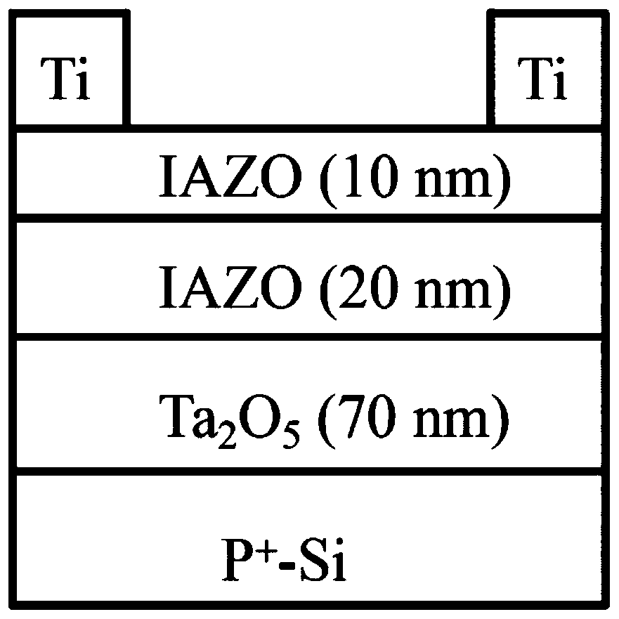
[0067] An indium aluminum zinc oxide thin film transistor based on a high dielectric constant gate dielectric layer, including P + -Si substrate, Ta 2 o 5 Gate dielectric layer, double active layer, source electrode and drain electrode, the double active layer includes the first layer of IAZO film and the second layer of IAZO film arranged in sequence from bottom to top, and the source electrode and drain electrode are grown on the second layer on IAZO film.

[0068] Ta 2 o 5 Has a high dielectric constant, Ta 2 o 5 The dielectric constant of SiO is about 2 six times the dielectric constant, so Ta 2 o 5 The gate voltage has a stronger ability to regulate carriers, and the required operating voltage is smaller, which can effectively improve the TFT operating voltage, field effect mobility, sub-threshold swing and other characteristic parameters.

[0069] Ta 2 o 5 The thickness of the gate dielectric layer is 50-150nm;

[0070] Ta of different thickness 2 o 5 The g...

Embodiment 2

[0076] According to an indium aluminum zinc oxide thin film transistor based on a high dielectric constant gate dielectric layer provided in Embodiment 1, the difference lies in:

[0077] Ta 2 o 5 The thickness of the gate dielectric layer is 70nm.

[0078] The thickness of the first layer of IAZO film is 20nm; the thickness of the second layer of IAZO film is 10nm.

[0079] Dimensions of the channel between the source electrode and the drain electrode: 2000 μm in width and 60 μm in length.

Embodiment 3

[0081] The full room temperature preparation method of the indium aluminum zinc oxide thin film transistor based on the high dielectric constant gate dielectric layer provided in embodiment 2 includes:

[0082] (1) at P + -Grow Ta on Si substrate 2 o 5 gate dielectric layer;

[0083] (2) at Ta 2 o 5 growing the first layer of IAZO film on the gate dielectric layer;

[0084] (3) growing a second layer of IAZO film on the first layer of IAZO film;

[0085] (4) Use electron beam evaporation to grow source and drain electrodes on the second layer of IAZO thin film.

[0086] In step (1), P + -Si substrate is a polished substrate, P + - Before using the Si substrate, use Decon (Decon) cleaning agent, deionized water, acetone, and ethanol in sequence on the P + -Si substrates were cleaned and dried with nitrogen gas.

[0087] The surface of the substrate has been polished, which is conducive to the growth of Ta with high flatness. 2 o 5 gate dielectric, and P + -Si subst...


PUM

PropertyMeasurementUnit
thicknessaaaaaaaaaa
thicknessaaaaaaaaaa
thicknessaaaaaaaaaa

Abstract

The invention relates to an indium aluminum zinc oxide thin film transistor based on a gate dielectric layer with high dielectric constant and a full room temperature preparation method thereof. The indium aluminum zinc oxide thin film transistor includes a P<+>-Si substrate, a Ta2O5 gate dielectric layer, double active layers, a source electrode and a drain electrode which are arranged in turn from bottom to top. The preparation method includes the following steps: (1) growing a Ta2O5 gate dielectric layer on a P<+>-Si substrate; (2) growing a first layer of IAZO film on the Ta2O5 gate dielectric layer; (3) growing a second layer of IAZO film on the first layer of IAZO film; and (4) growing a source electrode and a drain electrode on the second layer of IAZO film. An IAZO TFT with excellent performance is prepared in a room temperature environment by exploring and optimizing the sputtering preparation conditions of the Ta2O5 gate dielectric layer. The prepared IAZO TFT shows extremelyhigh electrical performance, and has a broad application prospect in flexible display and integrated circuits in the future.

Description

technical field [0001] The invention relates to an indium aluminum zinc oxide thin film transistor based on a high dielectric constant gate dielectric layer and a full room temperature preparation method thereof, belonging to the technical field of semiconductor materials and devices. Background technique [0002] With the rapid development of the microelectronics industry, the integration of electronic chips is getting higher and higher and the corresponding size is getting smaller and smaller. When the feature size of VLSI is less than or equal to 65nm, traditional silicon dioxide (SiO 2 ) The thickness of the gate dielectric layer needs to be less than 1.4nm, and such a thin SiO 2 Layers can greatly increase the device power dissipation of a transistor and reduce its gate voltage's ability to regulate the channel. It has been found that when the equivalent oxide layer thickness remains unchanged, the use of high dielectric constant (high k) materials to replace the trad...

Claims


Application Information

Patent Timeline
Patent Type & Authority Applications(China)
IPC IPC(8): H01L29/786H01L21/336
CPCH01L29/66742H01L29/786H01L29/78606
Inventor 冯先进徐伟东
Owner SHANDONG UNIV
Learn More