Crystal growth device and method

A technology of crystal growth and growth furnace, applied in the directions of crystal growth, single crystal growth, single crystal growth, etc., can solve the problems such as restricting the preparation period of SiC crystal, volatile components or impurities, and easy destruction of SiC seed crystal.

Active Publication Date: 2019-10-08
安徽微芯长江半导体材料有限公司
View PDF8 Cites 3 Cited by
  • Summary
  • Abstract
  • Description
  • Claims
  • Application Information

AI Technical Summary

Problems solved by technology

[0004] When the PVT method is used to grow SiC crystals, the high-temperature pretreatment of the raw materials is usually in the case of an axial temperature gradient in the growth chamber, which will cause the early unstable components or impurities to easily volatilize to the seeds if the treatment temperature is too high. The surface of the crystal will be polluted and destroyed, and if the treatment temperature is too low, the effect of removing impurities from the raw material will not be complete
In addition, a single slow or fast cooling and pressure drop is often selected in the seeding stage of cooling and pressure, which will easily lead to unstable and consistent volatile components deposited on the seed crystal, so that not only is it easy to form polytype inclusions but also aggregate on the growth interface. Thermal stress, which affects crystal quality and yield
SiC seed crystals are easily damaged in the early seeding stage of SiC crystal growth in the existing PVT method, and the thickness of the seed crystals must be controlled above 500 μm
However, the thickness of the large-size (especially 4 inches and above) commercial SiC wafers currently available on the market is 350 μm, which seriously restricts the preparation cycle of SiC crystals above 4 inches.

Method used


Image

  • Crystal growth device and method
  • Crystal growth device and method

Examples


Embodiment 1

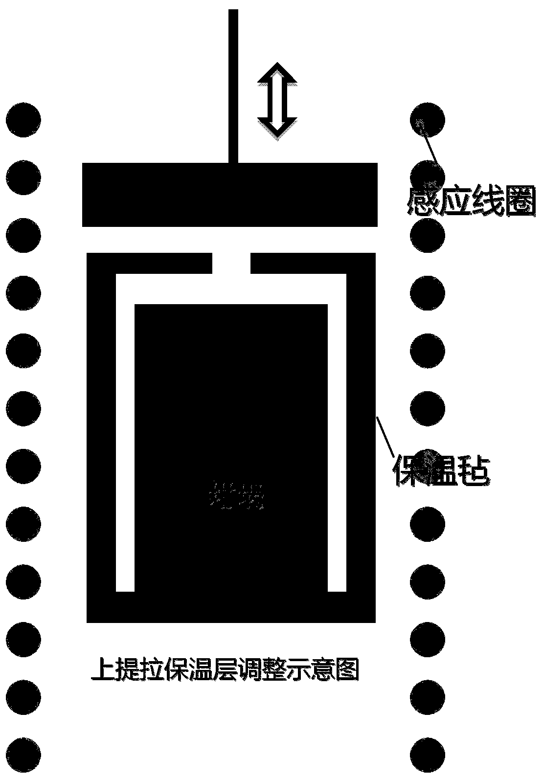
[0042] First, the graphite crucible with a diameter of 4 inches and a thickness of 400 μm seed crystal is fixed on the upper part, and the graphite crucible with silicon carbide raw material in the bottom material area is placed in the thermal insulation carbon felt (peripheral thermal insulation layer) (as a growth chamber). Place the above growth chamber in the crystal growth furnace, and pump the vacuum to 2.0×10 -4 Pa, filled with argon gas to a pressure of 10Torr, the upper insulation layer on the top of the furnace is slowly lowered until it covers the growth chamber through the lifting device on the furnace body, and the heating power is increased to 5kW to pretreat the raw materials for 3 hours, and then passed through the upper The pulling device slowly (1cm / min) pulls the insulation layer to the top of the growth furnace, and at the same time increases the heating power to 9.5kW and fills it with argon to 400Torr, keeps it for 3 hours, and then starts to lower the tem...

Embodiment 2

[0044] First, the upper part is fixed with a graphite cover with a diameter of 6 inches and a seed crystal thickness of 350 μm, and the graphite crucible with silicon carbide raw materials in the bottom material area is placed in an insulating carbon felt, and the above growth chamber is placed in a crystal growth furnace. Draw to 1.5×10 -4 Pa, filled with argon gas to a pressure of 200 Torr, slowly lower the insulation layer on the top until it covers the growth chamber through the lifting device on the furnace body, and at the same time increase the heating power to 8kW to pretreat the raw materials for 5 hours, and then pass the lifting device on the furnace body The pulling device slowly (0.5cm / min) pulls the upper insulation layer to the top of the growth furnace, and at the same time increases the heating power to 12.7kW and fills argon to 500Torr, and keeps it for 3.5 hours, and then starts to lower the temperature and pressure. First, the second The first stage took 0....


PUM


Abstract

The invention relates to a crystal growth device and method. The crystal growth device comprises a graphite crucible, a peripheral heat-preservation layer, a growth furnace and an upper heat-preservation layer, wherein the graphite crucible is provided with a graphite top cover, the bottom of the graphite crucible is used for storing polycrystal raw materials, and seed crystals are fixed to the side, facing the bottom, of the graphite top cover; the peripheral heat-preservation layer wraps the periphery of the graphite crucible but keeps at least part of the graphite top cover exposed; the graphite crucible wrapped with the peripheral heat-preservation layer is placed on the lower part of the growth furnace, a plurality of induction coils used for adjusting the temperature in the growth furnace are arranged at the inner periphery of the lower part of the growth furnace, and the growth furnace is further provided with an inflating and deflating connector so as to be selectively connected with a vacuum source or an inert gas source; and the upper heat-preservation layer is arranged on the graphite crucible and can ascend and descend.

Description

technical field [0001] The invention relates to a crystal growth device and a crystal growth method, in particular to a method for protecting seed crystals during the seeding stage of crystal growth, in particular to a method for protecting seed crystals during the seeding stage of silicon carbide crystal growth based on a physical vapor transport method, belonging to silicon carbide material field. Background technique [0002] Silicon carbide (SiC) single crystal material has the advantages of large band gap, high thermal conductivity, high electron saturation drift rate, high critical breakdown electric field, low dielectric constant, and good chemical stability. High-frequency high-power devices and ideal semiconductor materials for power electronic devices are widely used in white light lighting, optical storage, screen display, aerospace, high-temperature radiation environment, oil exploration, automation, radar and communication, and automotive electronics. [0003] ...

Claims


Application Information

Patent Timeline
IPC IPC(8): C30B23/00C30B29/36
CPCC30B23/00C30B29/36
Inventor 高攀忻隽孔海宽刘学超施尔畏
Owner 安徽微芯长江半导体材料有限公司
Why Eureka
Try Eureka