Surface plasmon enhanced LED optical communication device and manufacturing method thereof

A surface plasmon, optical communication technology, applied in the field of visible light communication, can solve the problems of low modulation bandwidth, low efficiency of LED light source, shortage, etc., and achieve the effect of enhancing modulation bandwidth, improving light source efficiency, and low cost

Inactive Publication Date: 2019-10-08
NANJING UNIV
View PDF7 Cites 7 Cited by
  • Summary
  • Abstract
  • Description
  • Claims
  • Application Information

AI Technical Summary

Problems solved by technology

[0004] The purpose of the present invention is to overcome the problems of low efficiency of LED light source and insufficient low modulation bandwidth in the existing optical communication,...

Method used


Image

  • Surface plasmon enhanced LED optical communication device and manufacturing method thereof
  • Surface plasmon enhanced LED optical communication device and manufacturing method thereof
  • Surface plasmon enhanced LED optical communication device and manufacturing method thereof

Examples


Embodiment 1

[0052] The preparation method of the surface plasmon enhanced LED optical communication device comprises the steps of:

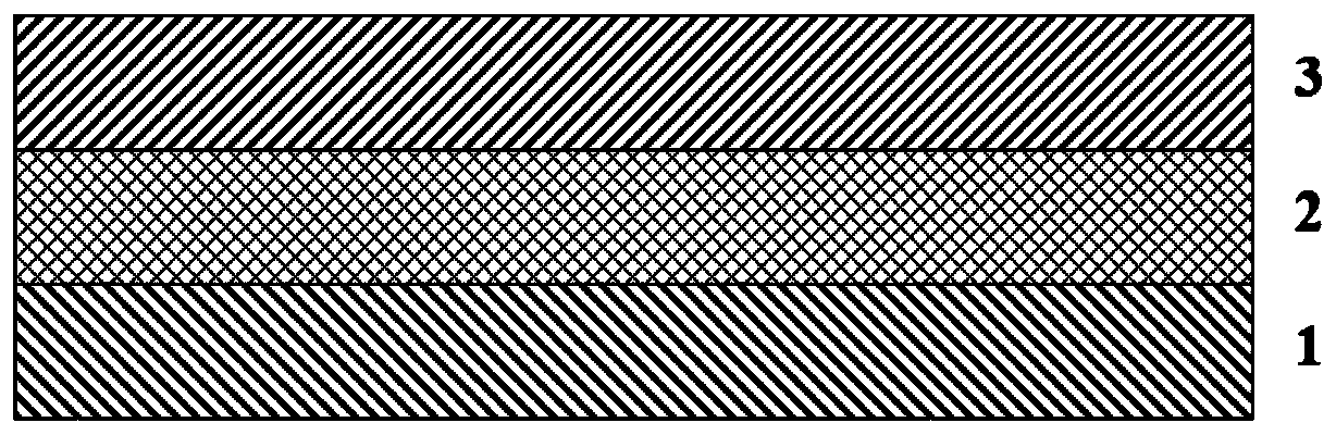
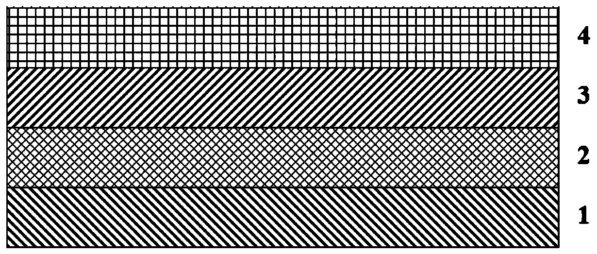
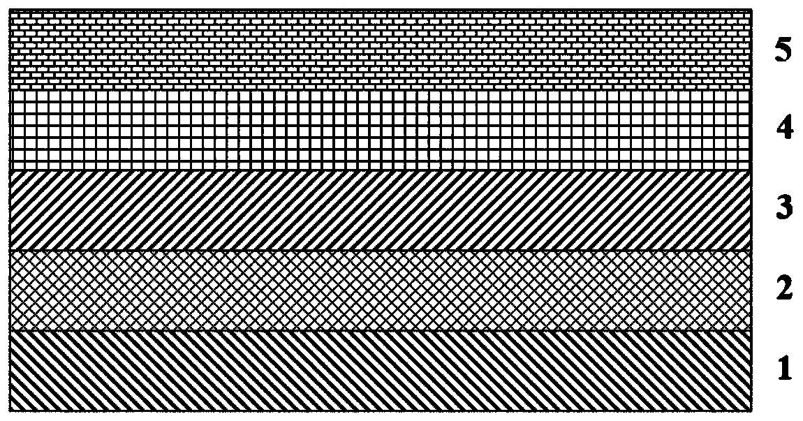
[0053] (1) Select a green light InGaN epitaxial wafer, the thickness of the N-type GaN layer 1 is 2um, the electron blocking layer 200nm, and the thickness of the P-type GaN layer 3 is 500nm; x Ga 1-x The period number of the N / GaN quantum well active layer 2 is 10, the In composition is 0.3, and the emission wavelength is 510nm. The thickness of the InGaN well layer is 3nm, and the thickness of the GaN barrier layer is 12nm.

[0054] (2) Using PECVD technology to grow a dielectric layer SiO on the surface of the substrate 2 , with a thickness of 100nm.

[0055] (3) Evaporating a Ni metal film with a thickness of 30 nm by using electron beam evaporation technology.

[0056] (4) Perform high-temperature heat treatment on the above-mentioned metal vapor-deposited substrate, and perform annealing in a high-temperature and high-purity nitrogen environment to ...

Embodiment 2

[0067] The preparation method of the surface plasmon enhanced LED optical communication device comprises the steps of:

[0068] (1) Select a green light InGaN epitaxial wafer, the thickness of the N-type GaN layer 1 is 2um, the electron blocking layer 200nm, and the thickness of the P-type GaN layer 3 is 500nm; x Ga 1-x The period number of the N / GaN quantum well active layer 2 is 10, the In composition is 0.3, and the emission wavelength is 510nm. The thickness of the InGaN well layer is 3nm, and the thickness of the GaN barrier layer is 12nm.

[0069] (2) Using PECVD technology to grow a dielectric layer SiO on the surface of the substrate 2 , with a thickness of 100nm.

[0070] (3) Evaporating a Ni metal film with a thickness of 30 nm by using electron beam evaporation technology.

[0071] (4) Perform high-temperature heat treatment on the above-mentioned metal vapor-deposited substrate, and perform annealing in a high-temperature and high-purity nitrogen environment to ...

Embodiment 3

[0081] The preparation method of the surface plasmon enhanced LED optical communication device comprises the steps of:

[0082] (1) Select a green light InGaN epitaxial wafer, the thickness of the N-type GaN layer 1 is 2um, the electron blocking layer 200nm, and the thickness of the P-type GaN layer 3 is 500nm; x Ga 1-x The period number of the N / GaN quantum well active layer 2 is 10, the In composition is 0.3, and the emission wavelength is 510nm. The thickness of the InGaN well layer is 3nm, and the thickness of the GaN barrier layer is 12nm.

[0083] (2) Using PECVD technology to grow a dielectric layer SiO on the surface of the substrate 2 , with a thickness of 100nm.

[0084] (3) Evaporating a Ni metal film with a thickness of 30 nm by using electron beam evaporation technology.

[0085] (4) Perform high-temperature heat treatment on the above-mentioned metal vapor-deposited substrate, and perform annealing in a high-temperature and high-purity nitrogen environment to ...


PUM

PropertyMeasurementUnit
Diameteraaaaaaaaaa
Heightaaaaaaaaaa
Luminous wavelengthaaaaaaaaaa

Abstract

The invention discloses a surface plasmon enhanced LED optical communication device. An array type nanopillar structure penetrating through a dielectric layer and a p-type GaN layer and stretching into an electron blocking layer is formed on an InGaN epitaxial wafer, nanopillars are filled with metal nanoparticles, or metal films are coated on sidewalls of the nanopillars. The invention further discloses a manufacturing method of the surface plasmon enhanced LED optical communication device. The metal surface plasmon effect is utilized to improve efficiency of an LED light source and enhance modulation bandwidth of optical communication, the nanostructure is prepared by PVD evaporation, high temperature heat treatment, RIE and ICP techniques, the secondary evaporation metal resonance wavelength is matched with the light emitting wavelength of multiple quantum wells, a metal period, the type, the size, the concentration, etc. are corrected in matching with the life spectrum test result,and carriers in a plasmon coupling state are eventually reduced to a picosecond scale. The surface plasmon enhanced LED optical communication device is advantaged in that efficiency of the LED lightsource can be effectively improved, the modulation bandwidth of optical communication is enhanced, the process is relatively simple, cost is low, and reliability is high.

Description

technical field [0001] The invention relates to a surface plasmon enhanced LED optical communication device and a preparation method thereof, belonging to the field of visible light communication. Background technique [0002] With the increasing number of smart devices, the demand for data transmission will increase explosively, but the transmission rate of the access network is still a "bottleneck" problem. Traditional wireless networks based on radio frequency and cellular networks have low transmission efficiency, high construction and maintenance costs, and will not be able to meet the huge communication needs in the future. Facing the increasing communication demands, LED-based visible light wireless communication technology (Visible Light Communication, VLC technology) has unique advantages. As a new wireless communication method, VLC technology has the advantages of high speed, anti-interference, energy saving, and high security. This technology uses indoor lightin...

Claims


Application Information

Patent Timeline
IPC IPC(8): H01L33/20H01L33/04H01L33/00B82Y40/00
CPCB82Y40/00H01L33/0075H01L33/04H01L33/20
Inventor 陶涛智婷刘斌谢自力陈鹏陈敦军修向前赵红张荣
Owner NANJING UNIV
Why Eureka
Try Eureka