Conductive composite and preparation method and application thereof
A conductive composite material and conductive material technology, applied in the field of flexible electronic materials, can solve the problems of poor conductivity, poor bonding force, and easy falling off of conductive materials, and achieve good durability and repeatability, enhanced bonding force, and hysteresis insignificant effect
- Summary
- Abstract
- Description
- Claims
- Application Information
AI Technical Summary
Problems solved by technology
Method used
Image
Examples
Embodiment 1
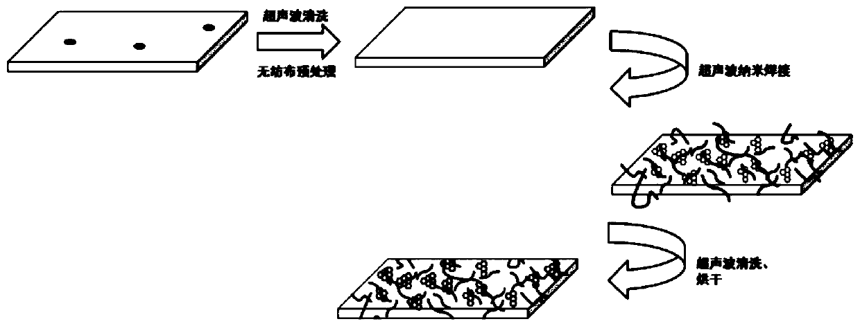
[0059] This embodiment is the preparation of conductive composite material carbon nanotube-graphene / non-woven fabric. For specific preparation steps, please refer to figure 2 :
[0060] (1) Cleaning of non-woven fabrics: in deionized water at 60°C, ultrasonic cleaning was performed on the non-woven fabrics for 5 minutes at a frequency of 20 kHz.
[0061] (2) Non-woven fabric pretreatment: Dry the non-woven fabric saturated with isopropanol at 60°C for 12 hours, cut the NWF with a thickness of 150 μm into substrates with a size of 1.3 cm×2.6 cm for use.
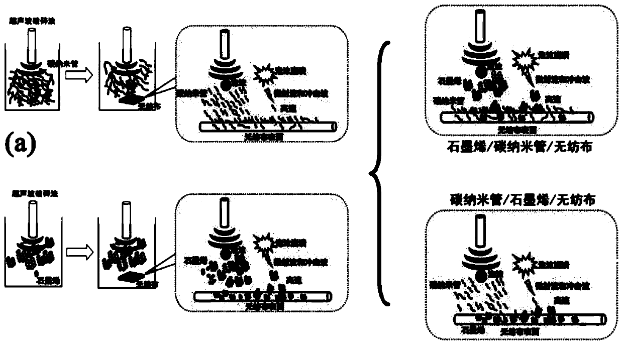
[0062] (3) Ultrasonic nano-welding: In the first step, mix sodium dodecyl sulfate with a mass ratio of 1:10 and multi-walled carbon nanotubes (MWCNTs) or graphene (rGO) in a beaker, and then inject a volume fraction of 25% isopropanol in deionized water solvent, and the whole system was ultrasonically dispersed for 30 minutes to obtain a multi-walled carbon nanotube dispersion / graphene dispersion (0.1mg / ml);
[0063] In the...
Embodiment 2
[0068] This embodiment is the preparation of a flexible stress sensing device.
[0069] Adopt magnetron sputtering technology to prepare cross Cu electrode array on the surface of carbon nanotube-graphene / non-woven fabric provided in embodiment 1 by mask plate, then use silver paste to weld two copper wires on carbon nanotube-graphene / both sides of the non-woven fabric to obtain a flexible stress sensor, wherein the process parameters are sputtering power of 10W; gas flow of pure argon gas of 10sccn; air pressure of 0.5Pa; deposition time of 30min.
[0070] Figure 4 Schematic diagram of the structure of the flexible stress sensing device provided by Embodiment 2 of the present invention. Such as Figure 4 As shown, the structure of the flexible stress sensing device of the present invention includes: non-woven fabric substrate 1 , multi-walled carbon nanotubes 2 , graphene 3 , crossed Cu electrode array 4 , and copper wire 5 . The multi-walled carbon nanotubes 2 are fuse...
PUM
| Property | Measurement | Unit |
|---|---|---|
| glass transition temperature | aaaaa | aaaaa |
| length | aaaaa | aaaaa |
| glass transition temperature | aaaaa | aaaaa |
Abstract
Description
Claims
Application Information


