Preparation method of silicon epitaxial wafer for high-voltage power device
A high-voltage power device, silicon epitaxial wafer technology, applied in semiconductor/solid-state device manufacturing, electrical components, gaseous chemical plating, etc., can solve the problems of high defect density, discrete thickness distribution, uncontrolled resistivity, etc. The effect of reducing the disturbance effect of resistivity and reducing the high temperature heating time
- Summary
- Abstract
- Description
- Claims
- Application Information
AI Technical Summary
Problems solved by technology
Method used
Image

Examples
Embodiment 1
[0032] (1) Heat the base of the reaction chamber, set the temperature to 1180 °C, flow in hydrogen chloride gas for etching, set the flow rate to 18 L / min, and set the etching time to 240 sec. The residual substances deposited in the early stage of the base were removed by etching, and then the reaction chamber was purged with a large flow rate of 90 L / min hydrogen to remove the impurities etched from the base from the reaction chamber, and then the base was cleaned. Cool down to 60°C.
[0033] (2) Install the silicon substrate on the base of the reaction chamber, raise the temperature of the silicon substrate to 1180 °C, and introduce low-flow hydrogen chloride gas into the reaction chamber, set the flow rate of hydrogen chloride to 0.8 L / min, and set the polishing time to 15 sec, the surface of the silicon substrate is polished.
[0034] (3) The reaction chamber was purged with a large flow rate of 90 L / min of hydrogen, and the purge time was set at 5 min to remove the impu...
Embodiment 2
[0043] (1) Heat the base of the reaction chamber, set the temperature to 1180 °C, flow in hydrogen chloride gas for etching, set the flow rate to 18 L / min, and set the etching time to 240 sec. The residual substances deposited in the early stage of the base were removed by etching, and then the reaction chamber was purged with a large flow rate of 90 L / min hydrogen to remove the impurities etched from the base from the reaction chamber, and then the base was cleaned. Cool down to 60°C.
[0044] (2) Install the silicon substrate on the base of the reaction chamber, raise the temperature of the silicon substrate to 1160 °C, and introduce low-flow hydrogen chloride gas into the reaction chamber, set the flow rate of hydrogen chloride to 1.0 L / min, and set the polishing time to 15 sec, the surface of the silicon substrate is polished.
[0045] (3) The reaction chamber was purged with a large flow rate of 90 L / min of hydrogen, and the purge time was set at 5 min to remove the impu...
Embodiment 3
[0054] (1) Heat the base of the reaction chamber, set the temperature to 1180 °C, flow in hydrogen chloride gas for etching, set the flow rate to 18 L / min, and set the etching time to 240 sec. The residual substances deposited in the early stage of the base were removed by etching, and then the reaction chamber was purged with a large flow rate of 90 L / min hydrogen to remove the impurities etched from the base from the reaction chamber, and then the base was cleaned. Cool down to 60°C.
[0055] (2) Install the silicon substrate on the base of the reaction chamber, raise the temperature of the silicon substrate to 1160°C, inject low-flow hydrogen chloride gas into the reaction chamber, set the flow rate of hydrogen chloride to 1.2 L / min, and set the polishing time to 15 sec, the surface of the silicon substrate is polished.
[0056] (3) The reaction chamber was purged with a large flow rate of 90 L / min of hydrogen, and the purge time was set at 5 min to remove the impurities v...
PUM
| Property | Measurement | Unit |
|---|---|---|
| thickness | aaaaa | aaaaa |
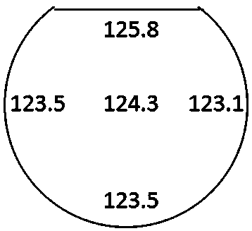
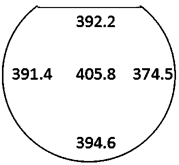
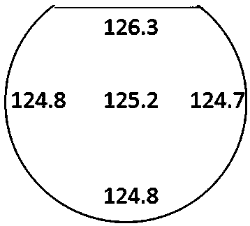
| electrical resistivity | aaaaa | aaaaa |
| diameter | aaaaa | aaaaa |
Abstract
Description
Claims
Application Information