LED epitaxial growth method

A technology of epitaxial growth and growth pressure, applied in electrical components, circuits, semiconductor devices, etc., can solve the problems of large warpage of epitaxial wafers and low luminous efficiency, and achieve the advantages of increasing window, reducing warpage and eliminating stress accumulation effect. Effect

Active Publication Date: 2019-10-25
XIANGNENG HUALEI OPTOELECTRONICS
View PDF11 Cites 3 Cited by
  • Summary
  • Abstract
  • Description
  • Claims
  • Application Information

AI Technical Summary

Problems solved by technology

After the LED size is upgraded to 4 inches, LEDs generally have technical pr

Method used


Image

  • LED epitaxial growth method
  • LED epitaxial growth method
  • LED epitaxial growth method

Examples


Embodiment 1

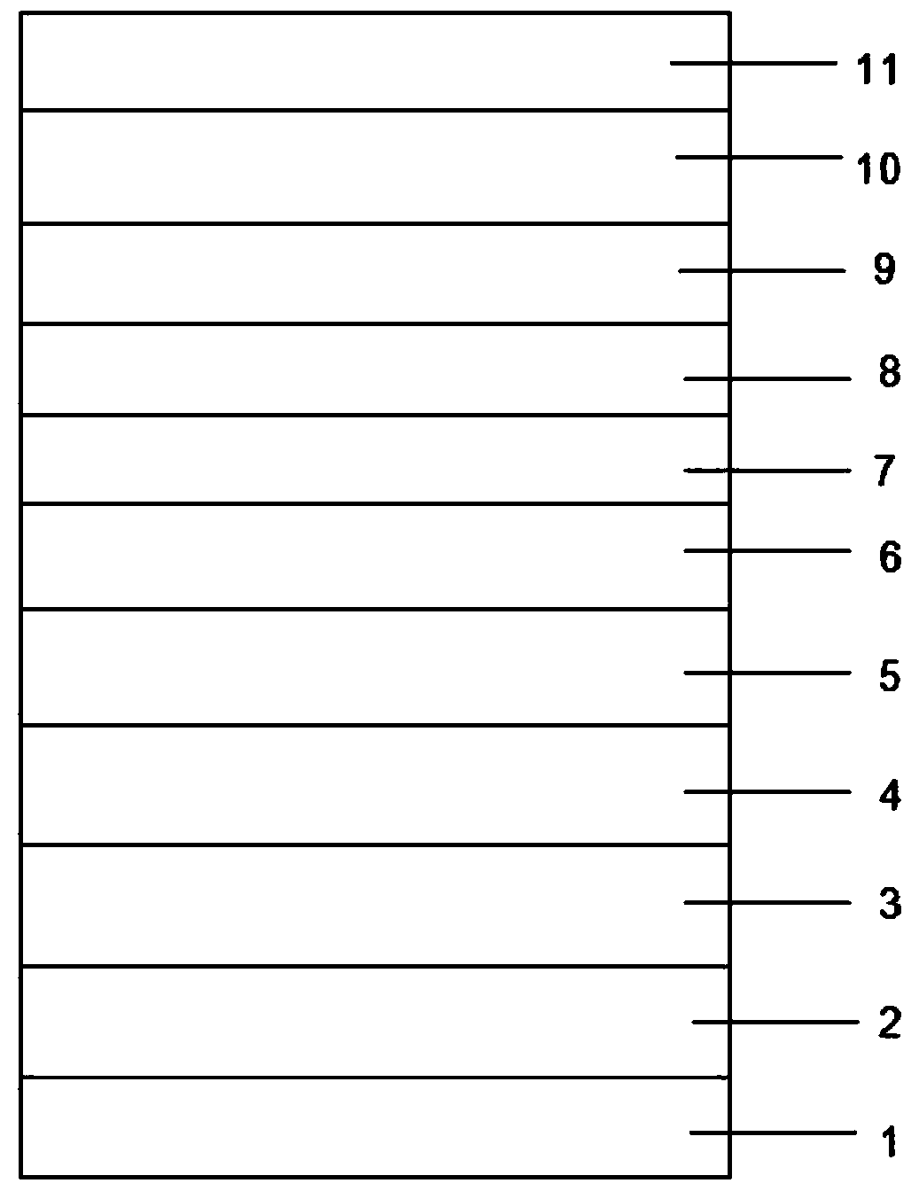
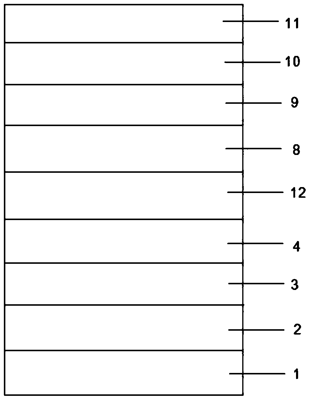
[0050] The application example of the LED epitaxial growth method of the present invention is provided below, and its epitaxial structure is shown in Fig. 1, figure 1 It is a schematic diagram of the structure of the LED epitaxial layer in the present invention, and the growth method can be found in figure 1 . This application uses VEECO MOCVD to grow high-brightness GaN-based LED epitaxial wafers. Using high-purity H 2 or high purity N 2 or high purity H 2 and high purity N 2 The mixed gas as the carrier gas, high-purity NH 3 (NH 3 Purity 99.999%) as N source, metal-organic trimethylgallium (TMGa) and metal-organic triethylgallium (TEGa) as gallium source, trimethylindium (TMIn) as indium source, N-type dopant as Silane (SiH 4 ), trimethylaluminum (TMAl) as the aluminum source, and the P-type dopant as magnesocene (CP 2 Mg), the substrate is (0001) sapphire, and the reaction pressure is between 100Torr and 1000Torr. The specific growth method is as follows:

[0051...


PUM

PropertyMeasurementUnit
Thicknessaaaaaaaaaa

Abstract

The invention discloses an LED epitaxial growth method, which sequentially comprises the steps of processing a substrate, growing a low-temperature nucleation layer GaN, growing a high-temperature GaNbuffer layer, growing an undoped u-GaN layer, growing an N2 and H2 mixed atmosphere low-temperature AlInGaN:Zn layer, growing an H2 atmosphere medium-temperature InGaN:Si layer, growing an N2 atmosphere high-temperature GaN:Mg layer, growing a light-emitting layer, growing a P-type AlGaN layer, growing a P-type GaN layer, growing a P-type GaN contact layer and cooling. Through introducing the structure of the N2 and H2 mixed atmosphere low-temperature AlInGaN:Zn layer, the H2 atmosphere medium-temperature InGaN:Si layer and the N2 atmosphere high-temperature GaN:Mg layer, the method disclosedby the invention improves the electron hole pairs in a light-emitting area of a quantum well, enhances the light-emitting radiation efficiency, improves the light-emitting efficiency of the LED and reduces the warpage of the epitaxial wafer.

Description

technical field [0001] The present application relates to the technical field of LED epitaxial design application, and in particular, relates to an LED epitaxial growth method. Background technique [0002] LED (Light Emitting Diode, Light Emitting Diode) is a kind of solid-state lighting. Its advantages such as small size, low power consumption, long service life, high brightness, environmental protection, and durability are recognized by consumers, and the scale of domestic production of LEDs is also gradually expanding; The demand for LED brightness and luminous efficiency is increasing day by day in the market. Customers are concerned that LEDs are more power-saving, have higher brightness and better luminous efficiency, which puts forward higher requirements for LED epitaxial growth. [0003] At present, the LED market now requires low driving voltage for LED chips, especially under high current, the smaller the driving voltage, the better, and the higher the light effi...

Claims


Application Information

Patent Timeline
IPC IPC(8): H01L33/00H01L33/06H01L33/12H01L21/02
CPCH01L33/007H01L33/06H01L33/12H01L21/0242H01L21/02458H01L21/02505H01L21/0254H01L21/0262
Inventor 徐平胡耀武龚彬彬黄胜蓝蒋东风
Owner XIANGNENG HUALEI OPTOELECTRONICS
Why Eureka
Try Eureka