Coupling structure and coupling method of semiconductor laser chip and silicon optical chip

A technology of silicon optical chip and coupling structure, which is applied in the direction of semiconductor lasers, lasers, laser components, etc., can solve the problems of unable to meet the needs of high power and high performance of light sources, low light output power of silicon-based light sources, complex processes, etc., to achieve Effects of reducing light field scattering loss, reducing light reflection, and flexible coupling

Inactive Publication Date: 2019-11-01
INST OF SEMICONDUCTORS - CHINESE ACAD OF SCI
View PDF11 Cites 16 Cited by
  • Summary
  • Abstract
  • Description
  • Claims
  • Application Information

AI Technical Summary

Problems solved by technology

However, the preparation of high-quality light source materials is complicated and immature. The monolithically integrated silicon-based light source has low light output power and poor RIN (relative intensity noise) noise, which cannot meet the needs of high-power and high-performance light sources in many applications.

Method used


Image

  • Coupling structure and coupling method of semiconductor laser chip and silicon optical chip
  • Coupling structure and coupling method of semiconductor laser chip and silicon optical chip

Examples


preparation example Construction

[0046] The invention also discloses a preparation method of the coupling structure as described above, which includes the following steps:

[0047] (1) setting an etching groove for coupling with the laser chip in the laser unit on the coupling end face of the silicon photonic chip to obtain a silicon photonic chip one;

[0048] (2) Set up spacers on the substrate of the laser unit where the silicon photonic chip needs to be connected;

[0049] (3) After aligning the active area of ​​the laser chip with the waveguide of silicon photonic chip 1, set a refractive index matching glue between the etching groove of the silicon photonic chip and the laser chip, and place it between the spacer and the silicon photonic chip Fixing glue is set to fix, and the coupling structure is obtained.

[0050] Wherein, the etching groove described in the step (1) is formed by a deep etching process;

[0051] Wherein, the laser unit described in step (2) comprises a substrate, a heat sink arrang...

Embodiment

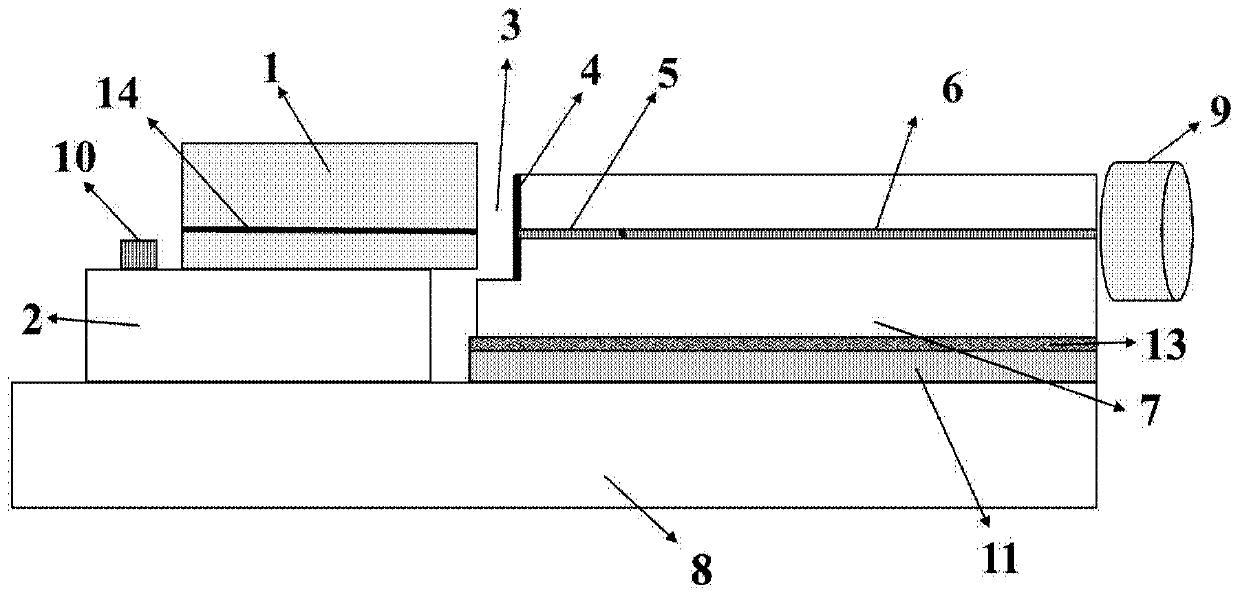
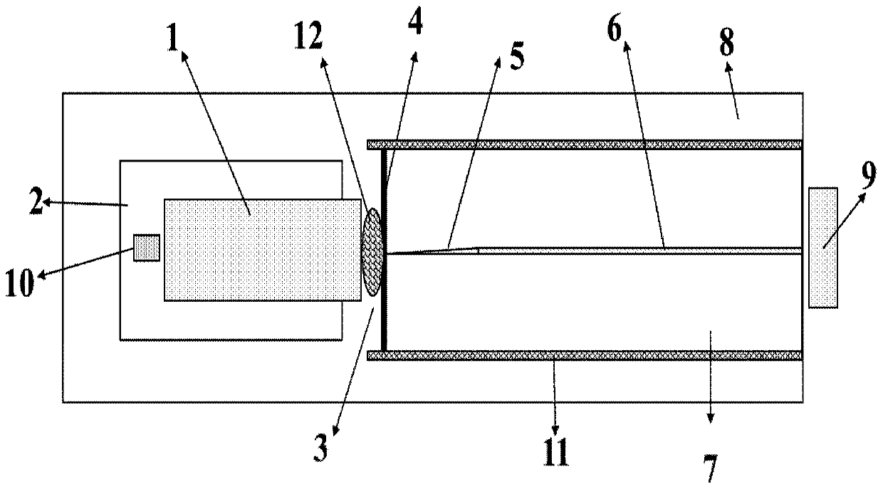
[0083] Such as figure 1 with figure 2 As shown, this embodiment provides a high-efficiency and low-loss coupling structure between a semiconductor laser chip and a silicon photonic chip, which includes a semiconductor laser chip 1 and a silicon photonic chip 7, wherein the silicon photonic chip 7 has a mode field conversion structure 5 And the waveguide structure 6 (including active and passive structures) on the silicon photonics chip 7 , heat sink 2 , thermistor 10 , spacer 11 , TEC substrate 8 , and high-sensitivity large-area detector 9 . The following are high-efficiency coupling methods and process implementation steps.

[0084] Step 1: Fabricate a silicon photonics chip 7 according to a conventional silicon photonics process, wherein the coupling end uses a deep etching process to form an etching groove 3 for end-face coupling, and a speckle conversion structure 5 is prepared at the coupling end, and a speckle conversion structure 5 The specific structure depends on ...


PUM


Abstract

The present invention provides a coupling structure and a coupling method of a semiconductor laser chip and a silicon optical chip. The coupling structure comprises: a laser unit comprising a laser chip; a silicon optical chip provided with a waveguide; and an etching groove arranged at the coupling end of the silicon optical chip and used for connecting with the laser unit and the silicon opticalchip. The coupling structure and the coupling method of the semiconductor laser chip and the silicon optical chip can achieve high-efficiency coupling of the semiconductor laser chip and the siliconoptical chip and facilitates providing of a high-quality light source for the silicon optical hybrid integration, an antireflection film is plated at the coupling end face of the silicon optical chip,the coupling loss and the RIN noise of the laser are reduced, the refractive index matching rubber fills the gap of the laser chip and the silicon optical chip, the scattering loss of the optical field is reduced, and the coupling loss is further reduced.

Description

technical field [0001] The disclosure belongs to the field of photon integration, and more specifically relates to a coupling structure and a coupling method of a semiconductor laser chip and a silicon photonic chip. Background technique [0002] One of the current development trends of optical communication is to achieve integration. Similar to integrated circuits, the optical communication system is integrated on a single optoelectronic chip. Only integration can achieve high density, low cost, and low energy consumption to meet the rapid expansion of information in the information society. . In recent years, silicon-based optoelectronic integration has achieved a series of exciting results, such as silicon-based optical waveguides, optical switches, modulators, and detectors have been realized, but the real silicon-based light source that can be used is still pending. This is mainly because silicon is an indirect bandgap semiconductor, and the radiative recombination pro...

Claims


Application Information

Patent Timeline
Patent Type & Authority Applications(China)
IPC IPC(8): H01S5/026G02B6/12
CPCG02B6/12004G02B2006/12085G02B2006/12121H01S5/026
Inventor 李金野刘建国戴双兴
Owner INST OF SEMICONDUCTORS - CHINESE ACAD OF SCI
Why Eureka
Try Eureka