A polymer-assisted epitaxial growth bifeo 3-δ Process for semiconducting thin films and products obtained therefrom

A polymer-assisted, epitaxial growth technology is applied in the field of epitaxial growth of BiFeO3-δ semiconducting thin films, which can solve the problems of difficult detection of semiconductor chips, and achieve the effects of good application potential, high electrical conductivity and good ferroelectricity.

Active Publication Date: 2021-08-24
UNIV OF JINAN
View PDF0 Cites 0 Cited by
  • Summary
  • Abstract
  • Description
  • Claims
  • Application Information

AI Technical Summary

Problems solved by technology

BiFeO 3 It has very good ferroelectric properties at room temperature, and it is the material with the smallest bandgap among ferroelectric materials, but its bandgap is also above 2.7eV, and the obtained maximum ferroelectric diode current is also lower than 20 mA cm -2 The order of magnitude belongs to the range that is not easy to detect in the current semiconductor chip detection technology

Method used


Image

  • A polymer-assisted epitaxial growth bifeo  <sub>3-δ</sub> Process for semiconducting thin films and products obtained therefrom
  • A polymer-assisted epitaxial growth bifeo  <sub>3-δ</sub> Process for semiconducting thin films and products obtained therefrom
  • A polymer-assisted epitaxial growth bifeo  <sub>3-δ</sub> Process for semiconducting thin films and products obtained therefrom

Examples


Embodiment 1

[0032] Semiconducting Ferroelectric BiFeO 3-δ The preparation of thin film, steps are as follows:

[0033] 1. Configuration of precursor solution

[0034] Bi(NO 3 ) 3 ∙5H 2 O solid powder was added to glacial acetic acid (CH 3 COOH) (Bi: glacial acetic acid molar ratio is 1:8), continuously stirred on a magnetic stirrer for 8 h, and kept the temperature at 40-50 °C until the solution was a transparent solution, and the Bi(NO 3 ) 3 ∙5H 2 Fe(NO 3 ) 3 ∙9H 2 O was added to the above solution, and continuously stirred on a magnetic stirrer for 2h until the Fe(NO 3 ) 3 ∙9H 2 After O is completely dissolved. Then add polyethylene glycol 20000, polyethylene glycol 400 and citric acid according to the molar ratio of bismuth ferrite: polyethylene glycol 20000: polyethylene glycol 400: citric acid=1: 0.01%: 0.01%: 1, and finally Add equal volume ratio of ethylene glycol and ethylene glycol methyl ether to dilute the solution to BiFeO 3 The concentration of the solution was...

Embodiment 2

[0042] Semiconducting Ferroelectric BiFeO 3-δ The preparation of thin film, steps are as follows:

[0043] 1. Configuration of precursor solution

[0044] With embodiment 1.

[0045] 2. Coating machine throwing film

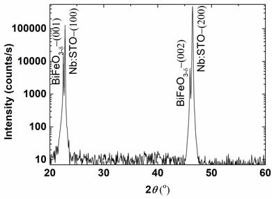
[0046] (100) Nb:SrTiO 3 The substrate is placed in a tube furnace at 700 o C under heat treatment for 30 minutes, then keep the temperature at 80 o C and put it into a homogenizer, keep the humidity range at 14-17%, then apply the precursor solution on the substrate, and prepare a single-layer film by spin coating; wherein, the first layer of film is thrown at a speed of 7000rpm , the time is 2 minutes, and the film thickness is about 11-16 nm; the second-third film is spun at a speed of 5000rpm, the time is 1 minute, the film thickness is about 20-25 nm, and the other layers are spun at a speed of 6000rpm film, the time is 1 minute, and the film thickness is guaranteed to be around 15-18 nm;

[0047] 3. Heat treatment

[0048] With embodiment 1.

[0049...

Embodiment 3

[0052] Semiconducting Ferroelectric BiFeO 3-δ The preparation of thin film, steps are as follows:

[0053] 1. Configuration of precursor solution

[0054] With embodiment 1.

[0055] 2. Coating machine throwing film

[0056] (100) Nb:SrTiO 3 The substrate is placed in a tube furnace at 700 o C under heat treatment for 30 minutes, then keep the temperature at 80 o C and put it into a homogenizer, keep the humidity range at 14-17%, then apply the precursor solution on the substrate, and prepare a single-layer film by spin coating; wherein, the first layer of film is thrown at a speed of 6000rpm , the time is 2 minutes, and the film thickness is about 14-18 nm; the second-third film is spun at a speed of 4000rpm, and the time is 1 minute, and the film thickness is about 23-28nm, and the other layers are spun at a speed of 5000rpm , the time is 1 minute, and the film thickness is guaranteed to be around 22-25;

[0057] 3. Heat treatment

[0058] With embodiment 1.

[0059...


PUM

PropertyMeasurementUnit
thicknessaaaaaaaaaa
thicknessaaaaaaaaaa
thicknessaaaaaaaaaa

Abstract

The invention discloses a polymer-assisted epitaxial growth of BiFeO 3‑δ The method for semiconducting thin film, comprising: preparing precursor solution, adopting layer-by-layer annealing process on the substrate to prepare thin film, the temperature of each layer of thin film preparation is 60-80°C, and the humidity is 11-15% when the film is flung, The thickness of the first film is 11-18 nm, the thickness of the second-third film is 20-28 nm, the thickness of the other films is 14-24 nm, and the annealing atmosphere is nitrogen. The method of the invention is easy to implement, does not have high requirements for experimental equipment, the stoichiometric ratio of raw materials can be precisely controlled, the process operation is simple and convenient, and the obtained film has both good ferroelectricity and high electrical conductivity. It has great application potential in non-volatile memory devices.

Description

technical field [0001] The invention relates to a kind of epitaxial growth BiFeO 3-δ A method for semiconducting thin films, specifically involving a polymer-assisted high-quality epitaxial growth of BiFeO 3-δ Process for semiconducting thin films and products obtained by the process. Background technique [0002] Ferroelectric capacitive memory cannot be extended to gigabit high-density devices due to its large cell area, and capacitive memory cells need to apply recovery voltage pulses to write data again after destructively reading data. The ferroelectric diode memory cell can realize bipolar switching between its high conductance state and low conductance state under two opposite ferroelectric polarization directions, and then can realize non-destructive readout of binary information. Compared with the traditional capacitive storage unit, the ferroelectric diode storage unit can be made into a very efficient size, so the storage density can be greatly improved. In add...

Claims


Application Information

Patent Timeline
Patent Type & Authority Patents(China)
IPC IPC(8): C23C26/00
CPCC23C26/00
Inventor 杨锋刘芬季凤岐林延凌
Owner UNIV OF JINAN
Why Eureka
Try Eureka