Boron process applicable for P+ selective emitter battery

An emitter and selective technology, applied in circuits, electrical components, climate sustainability, etc., can solve battery open circuit voltage and short circuit current limitations, high recombination of non-metallic electrode contact areas, boron selective doping and diffusion technology gaps and other problems, to achieve the effect of increasing the open circuit voltage and short circuit current, increasing the fill factor, and improving the ohmic contact

Active Publication Date: 2019-12-20
常州顺风太阳能科技有限公司
View PDF5 Cites 4 Cited by
  • Summary
  • Abstract
  • Description
  • Claims
  • Application Information

AI Technical Summary

Problems solved by technology

Among them, boron diffusion is widely used in N-type high-efficiency solar cells as an important means of p+ layer doping. The common method is to carry gas boron source into the furnace tube for single boron doping, but for boron selective doping diffusion technology is still blank
[0003] Moreover, th

Method used


Image

  • Boron process applicable for P+ selective emitter battery
  • Boron process applicable for P+ selective emitter battery

Examples


Embodiment 1

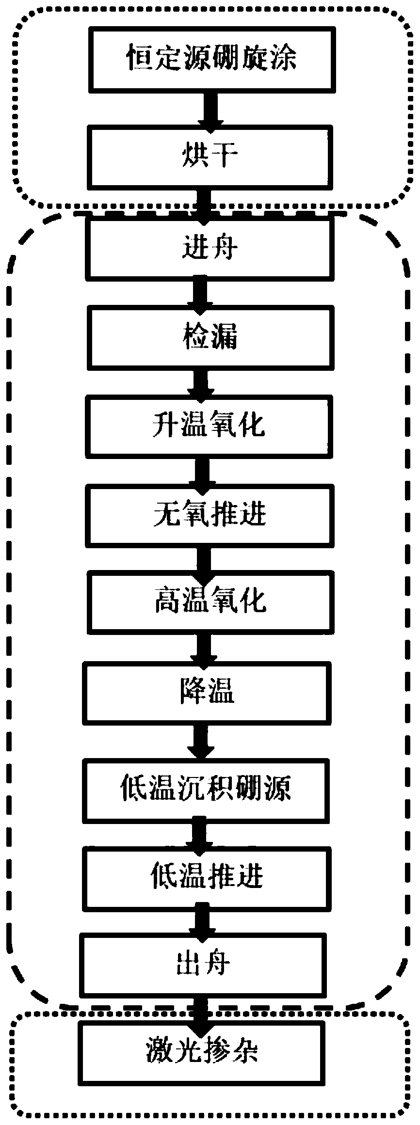
[0048] A constant source boron diffusion process suitable for P+ selective emitter batteries, the specific process is as follows: use N-type silicon wafers with high minority carrier life, resistivity 0.2-2Ω.cm, double-sided alkali washing for texture;

[0049] (1) Constant source boron spin-coating—use 1-1.5mL of immersion solution to spin on the silicon wafer, and then drop 0.4-0.8ml of boron source to spin on the silicon wafer. The spin coating method can produce a higher square resistance of 120-140 ohm, and the uniformity STD<8;

[0050] (2) Drying—on a chain machine at a temperature of 120-200°C and a drying time of 30-60s;

[0051] (3) Entering the boat - the temperature is maintained at 750-850°C, the nitrogen flow rate is 1000-2000sccm, and the time is about 8-15min;

[0052] (4) Leak detection - the flow rate of nitrogen gas is 1000-1500sccm, and the pressure is controlled at 100-200pa;

[0053] (5) Heating Oxidation—The temperature rises to 900-960°C, the nitrogen...

Embodiment 2

[0063] A constant source boron diffusion process suitable for P+ selective emitter batteries, the specific process is as follows: use N-type silicon wafers with high minority carrier life, resistivity 2-6Ω.cm, double-sided alkali-washed texture;

[0064] (1) Constant source boron spin-coating—use 1.5-2.5mL of immersion solution to spin on the silicon wafer by spin-coating, and then drop 0.3-0.6ml of boron source to spin on the silicon wafer. The spin coating method can produce a higher square resistance of 130-200 ohm, and the uniformity STD: 9-10;

[0065] (2) Drying—on a chain machine at a temperature of 180-250°C and a drying time of 40-80s;

[0066] (3) Entering the boat - the temperature is maintained at 750-850°C, the nitrogen flow rate is 1500-2500sccm, and the time is about 6-15min;

[0067] (4) Leak detection - the nitrogen flow rate is 1500-2500sccm, and the pressure is controlled at 100-200pa;

[0068] (5) Heating Oxidation—The temperature rises to 950-1000°C, the...


PUM

PropertyMeasurementUnit
Resistivityaaaaaaaaaa

Abstract

The invention relates to a boron process applicable for a P+ selective emitter battery. The boron process comprises the following steps of (1) performing constant source boron spinning; (2) drying; (3) allowing a boat to enter a furnace tube; (4) detecting leakage; (5) performing temperature-rising oxidization; (6) performing oxygen-free push; (7) performing high-temperature oxidization; (8) reducing a temperature; (9) performing low-temperature boron source deposition; (10) performing low-temperature push; (11) allowing the boat to get out; and (12) performing laser doping. By a joint effectof constant boron source boron push and gas boron source doping, on one hand, a light-doping region is formed, and an open-circuit voltage and a short-circuit current of the battery can be effectivelyincreased by a structure having a high surface concentration shallow junction; and on the other hand, a heavy-doping region is formed by secondary doping with laser, ohmic contact can be effectivelyimproved, and a filling factor is improved.

Description

technical field [0001] The invention relates to the field of solar cell manufacturing, in particular to a boron process suitable for P+ selective emitter cells. Background technique [0002] As the demand for affordable Internet access intensifies, high-efficiency batteries have become a development trend. Especially today's N-TOPCon batteries are getting more and more popular. However, how to raise the efficiency of N-TOPCon batteries to a higher level has become the focus of research and development. Among them, boron diffusion is widely used in N-type high-efficiency solar cells as an important means of p+ layer doping. The common method is to carry gas boron source into the furnace tube for single boron doping, but for boron selective doping diffusion technology is still blank. [0003] Moreover, the conventional boron diffusion process is required to form a good ohmic contact with the metal electrode, and the square resistance is low, which leads to high recombinatio...

Claims


Application Information

Patent Timeline
IPC IPC(8): H01L31/0224H01L31/18
CPCH01L31/022425H01L31/18H01L31/1828Y02P70/50
Inventor 瞿辉曹玉甲王芹芹
Owner 常州顺风太阳能科技有限公司
Why Eureka
Try Eureka