N-type nanometer black silicon manufacturing method and solar cell manufacturing method

A solar cell, N-type technology, applied in the direction of nanotechnology, nanotechnology, nanotechnology for materials and surface science, etc., can solve the problems of industrial application obstacles and high cost, and achieve the purpose of reducing corrosion depth, increasing lifespan, Effect of increasing short-circuit current and open-circuit voltage

Active Publication Date: 2015-03-11
ZHEJIANG JINKO SOLAR CO LTD
View PDF8 Cites 4 Cited by
  • Summary
  • Abstract
  • Description
  • Claims
  • Application Information

AI Technical Summary

Problems solved by technology

However, the high cost of TMAH has cau

Method used


Image

  • N-type nanometer black silicon manufacturing method and solar cell manufacturing method
  • N-type nanometer black silicon manufacturing method and solar cell manufacturing method
  • N-type nanometer black silicon manufacturing method and solar cell manufacturing method

Examples


Example Embodiment

[0045] Example 1

[0046] The preparation method of the N-type nano black silicon of the present embodiment comprises the steps:

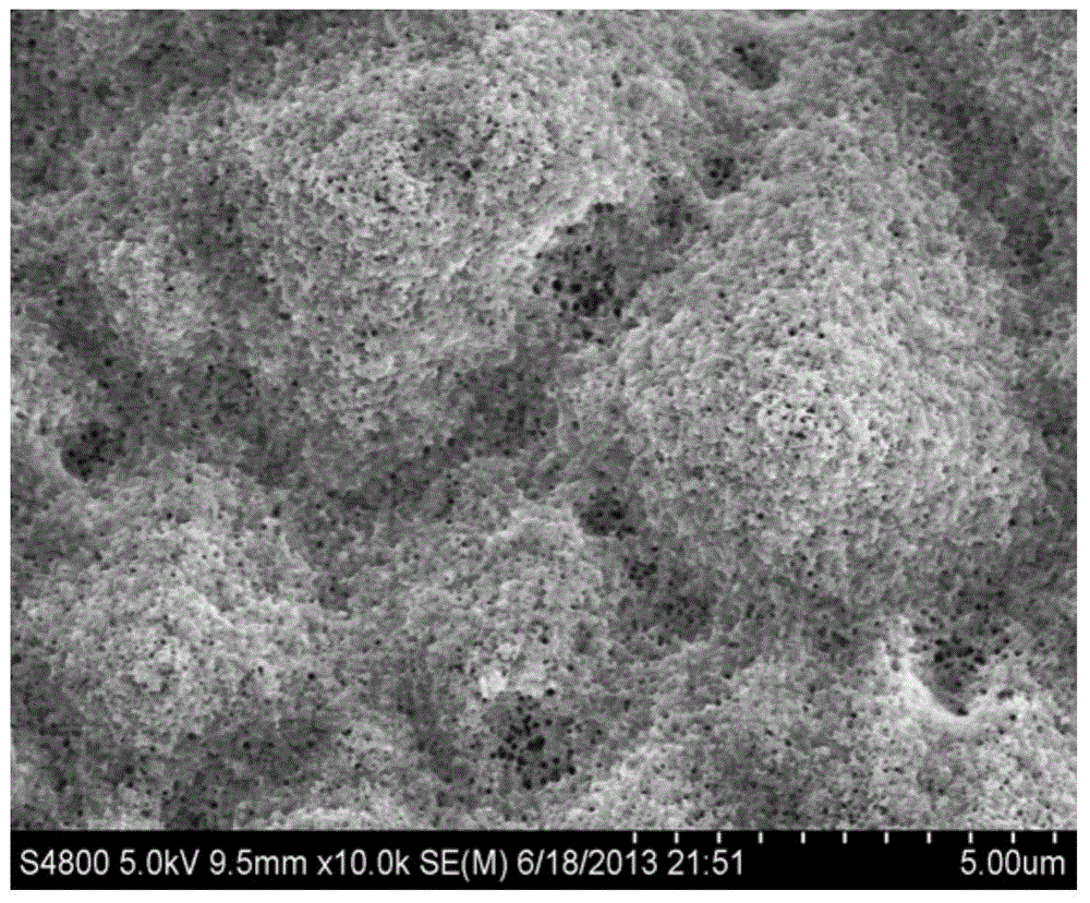
[0047] (1) 1.5g polyvinylpyrrolidone (PVP K-30) is dissolved in water, forms 50g base liquid, and the mass concentration of formaldehyde is 0.74% in the base liquid, and the mass concentration of polyvinylpyrrolidone in the base liquid is 3%, to base liquid Add dropwise silver nitrate aqueous solution mass concentration in the liquid to be 1.7%, rapidly inject ammonia water (mass fraction is 0.6ml of the solution of 28%), react 30min under 35 ℃, obtain the solution of silver nanoparticles, then add alcohol and centrifuge four times, obtain silver Nanoparticles, the silver nanoparticles are spherical, and the size (particle diameter) of the silver nanoparticles is 50nm-100nm.

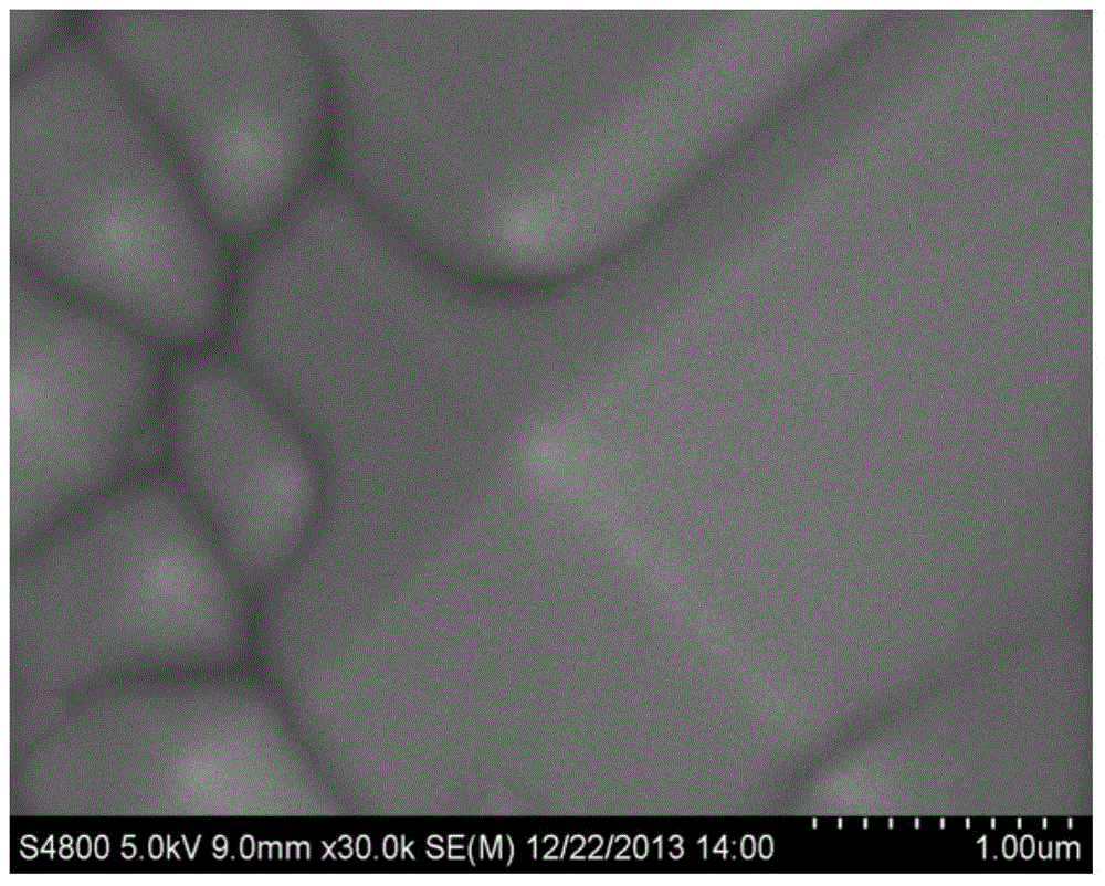
[0048] (2) Put an N-type silicon wafer (N-type Czochralski single-crystal native silicon wafer) with a size of 156mm×156mm into 20mt% KOH solution, react at 80°C for 2min, a...

Example Embodiment

[0062] Example 2

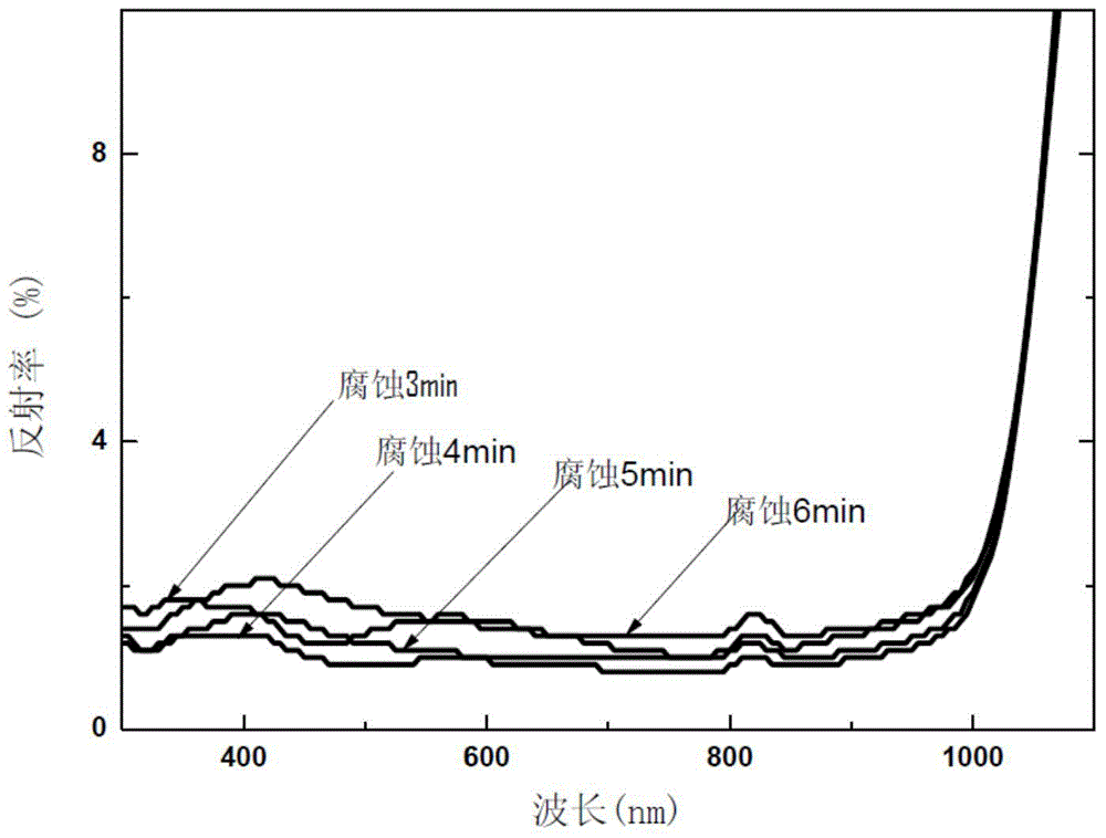
[0063] Same as Example 1, the difference is that the etching time in step (5) is 4min, and the N-type silicon wafer after step (5) is processed by the following process between step (6) and step (7) Make etch corrections:

[0064] Put the N-type silicon chip treated in step (6) into 2wt% NaOH solution and react for 3 minutes, so as to perform etching correction on the nano light-trapping structure obtained in step (5). Then put the silicon chip into 10vol% hydrochloric acid for 2 minutes to remove sodium ions, then clean the silicon chip with deionized water, and then dry it with nitrogen gas.

[0065] The nanometer black silicon N+NP solar cell prepared in Example 2 was tested for various electrical properties of the cell by using a cell efficiency sorter under the light intensity of AM 1.5, and the results are shown in Table 1.

[0066] The minority carrier lifetime of the N-type nano-black silicon prepared in this example is 5.19 μs, and the correspondi...


PUM

PropertyMeasurementUnit
Sizeaaaaaaaaaa
Life expectancyaaaaaaaaaa

Abstract

The invention discloses an N-type nanometer black silicon manufacturing method and a solar cell manufacturing method. The N-type nanometer black silicon manufacturing method comprises steps that: (1), silicon chips after cleaning react in mixed solution of KOH and isopropanol for 0.5-2 hours, and the reaction temperature is 60-100 DEG C; and (2), the N-type silicon chips treated in the step (1) are put in a silver nanometer particle solution for 20-30 minutes in a standing mode, after drying, corrosion treatment on the treated N-type silicon chips is carried out to acquire the N-type nanometer black silicon. For manufacturing a solar cell, an N+ layer, a silicon nitride layer and an electrode layer are sequentially formed at the front surface of the manufactured N-type nanometer black silicon, after sintering, the N-type nanometer black silicon solar cell is manufactured. The manufactured N-type nanometer black silicon solar cell has properties of low reflectivity and high carrier service life and has the conversion efficiency 2.2% higher than that of a cell manufactured through a routine method.

Description

technical field [0001] The invention relates to the field of photovoltaic technology, in particular to a method for preparing N-type nano black silicon and a method for preparing solar cells. Background technique [0002] Optical loss is a major factor hindering the improvement of solar cell efficiency, and reducing the optical loss of solar cells is an important and effective way to improve cell efficiency. At present, crystalline silicon mainly adopts "pyramid" texture anti-reflection structure on the surface of silicon wafer to reduce the reflectivity, but its average reflectivity in the visible light band is above 10%, and the reflection loss of light is still relatively large, which restricts the efficiency of solar cells. Further improve. [0003] The nanoporous black silicon structure can effectively reduce the reflectivity of the anti-reflection structure. It can be prepared by electrochemical methods and metal-assisted catalysis. Metal-assisted catalysis has rece...

Claims


Application Information

Patent Timeline
IPC IPC(8): H01L31/18B82Y30/00
CPCB82Y30/00H01L31/18H01L31/186Y02E10/50Y02P70/50
Inventor 汪雷戴准庄重源王明昂张军娜唐勋杨德仁
Owner ZHEJIANG JINKO SOLAR CO LTD
Why Eureka
Try Eureka