Efficient crystalline silicon solar cell and production method thereof

A solar cell and crystalline silicon technology, applied in the field of solar cells, can solve the problems of inability to form ohmic contact between silver grid lines and silicon, low filling factor, and reduced phosphorus doping concentration, so as to improve photoelectric conversion efficiency, increase open circuit voltage and Effect of short circuit current

Inactive Publication Date: 2015-02-18
GUANGDONG AIKO SOLAR ENERGY TECH
View PDF5 Cites 3 Cited by
  • Summary
  • Abstract
  • Description
  • Claims
  • Application Information

AI Technical Summary

Problems solved by technology

[0004] like figure 1 As shown, the P-N junction of traditional solar cells is made by primary phosphorus doping. In order to increase the open circuit voltage and short circuit current of the battery, the only way to increase the overall diffusion resistance and reduce the phosphorus doping concentration, bu

Method used


Image

  • Efficient crystalline silicon solar cell and production method thereof
  • Efficient crystalline silicon solar cell and production method thereof
  • Efficient crystalline silicon solar cell and production method thereof

Examples


preparation example Construction

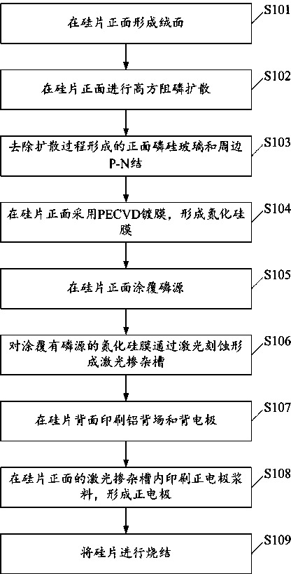
[0045] image 3 It is a flowchart of the preparation method of the high-efficiency crystalline silicon solar cell of the present invention, including:

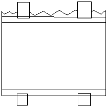
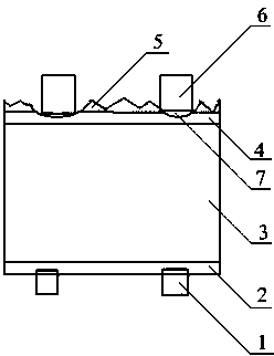
[0046] S101, forming a textured surface on the front side of the silicon wafer.

[0047] The front side of the silicon wafer is suede, which can reduce the surface reflectivity and increase the utilization rate of light.

[0048] S102, perform high resistance phosphorus diffusion on the front side of the silicon wafer, the diffusion resistance is 100~150Ω / □.

[0049] The use of high square resistance diffusion can achieve lower doping concentration, increase the open circuit voltage and short circuit current of the battery, thereby improving the photoelectric conversion efficiency of the battery.

[0050] S103 , removing the front phosphosilicate glass (PSG) and peripheral P-N junctions formed in the diffusion process.

[0051] S104, using PECVD (Plasma Enhanced Chemical Vapor Deposition, plasma enhanced chemical vapor depo...

Embodiment 1

[0076] Form a textured surface on the front side of the silicon wafer;

[0077] Perform high-resistance phosphorus diffusion on the front side of the silicon wafer, and the diffusion resistance is 150Ω / □;

[0078] Remove the front phosphosilicate glass and surrounding P-N junctions formed during the diffusion process;

[0079] PECVD coating is used on the front side of the silicon wafer to form a silicon nitride film with a thickness of 90nm;

[0080] Coating a phosphorus source on the front side of the silicon wafer by spin coating, the phosphorus source is a phosphoric acid solution with a phosphoric acid concentration of 10%;

[0081] A laser-doped groove is formed by laser etching on the silicon nitride film coated with a phosphorus source. The width of the laser-doped groove is 80 μm, so that phosphorus is doped into the silicon in the laser-doped groove. The groove pattern is a linear positive electrode grid pattern;

[0082] Print aluminum back field and back electro...

Embodiment 2

[0086] Form a textured surface on the front side of the silicon wafer;

[0087] Perform high-resistance phosphorus diffusion on the front side of the silicon wafer, and the diffusion resistance is 100Ω / □;

[0088] Remove the front phosphosilicate glass and surrounding P-N junctions formed during the diffusion process;

[0089] PECVD coating is used on the front side of the silicon wafer to form a silicon nitride film with a thickness of 75nm;

[0090] A phosphorus source is coated on the front side of the silicon wafer by spin coating, and the phosphorus source is a phosphoric acid solution with a phosphoric acid concentration of 1%.

[0091] A laser-doped groove is formed by laser etching on the silicon nitride film coated with a phosphorus source. The width of the laser-doped groove is 40 μm, so that phosphorus is doped into the silicon in the laser-doped groove. The groove pattern is a linear positive electrode grid pattern;

[0092] Print aluminum back field and back el...


PUM

PropertyMeasurementUnit
Widthaaaaaaaaaa
Widthaaaaaaaaaa
Thicknessaaaaaaaaaa

Abstract

The invention discloses an efficient crystalline silicon solar cell which comprises back electrodes, an aluminum back surface field, P type silicon, N type silicon, a silicon nitride film and positive electrodes. A phosphorus source coats the silicon nitride film, then laser doping grooves are formed in the silicon nitride film through laser etching, phosphorus is doped into the silicon in the laser doping grooves, and the laser doping grooves form a linear positive electrode grid line pattern. The bottoms of the positive electrodes are located in the laser doping grooves. The invention further discloses a method for producing the efficient crystalline silicon solar cell. The efficient crystalline silicon solar cell has the advantages that the laser doping grooves are formed through laser phosphorus source doping, phosphorus doping concentration on the surface of a silicon wafer is in selective distribution, the laser phosphorus doping concentration of the areas within grid lines is high, and good ohmic contact of the grid lines and the silicon is guaranteed; high sheet resistance diffusion is used to allow the doping concentration of areas outside the grid lines to be low, the open-circuit voltage and the short circuit currents of the solar cell are increased, and the photoelectric conversion efficiency of the solar cell is increased.

Description

technical field [0001] The invention relates to the technical field of solar cells, in particular to a high-efficiency crystalline silicon solar cell and a preparation method thereof. Background technique [0002] A solar cell is a device that effectively absorbs solar radiation energy and uses the photovoltaic effect to convert light energy into electrical energy. When sunlight shines on a semiconductor P-N junction (P-N Junction), a new hole-electron pair (V-E pair) is formed. , Under the action of the P-N junction electric field, holes flow from the N region to the P region, electrons flow from the P region to the N region, and a current is formed after the circuit is turned on. Because it is a solid semiconductor device that converts sunlight energy into electrical energy by using the photovoltaic effect of various potential barriers, it is also called a solar cell or a photovoltaic cell, and is an important component of a solar array power system. [0003] Solar cells ...

Claims


Application Information

Patent Timeline
IPC IPC(8): H01L31/04H01L31/0352H01L31/0216H01L31/18H01L21/318H01L21/22
CPCH01L21/22H01L31/02167H01L31/035272H01L31/06H01L31/18Y02E10/50Y02P70/50
Inventor 方结彬秦崇德石强黄玉平何达能
Owner GUANGDONG AIKO SOLAR ENERGY TECH
Why Eureka
Try Eureka