
Preparation method of perovskite passivation layer

A technology of passivation layer and perovskite, which is applied in semiconductor/solid-state device manufacturing, semiconductor devices, electrical components, etc., can solve problems such as unsatisfactory effects, and achieve improved quality, low defect state density, and good electrical properties.

Active Publication Date: 2019-12-27
JILIN NORMAL UNIV
View PDF4 Cites 4 Cited by
  • Summary
  • Abstract
  • Description
  • Claims
  • Application Information

AI Technical Summary

Problems solved by technology

Due to the large lattice mismatch and stress between perovskite and heterogeneous materials, the effect of this kind of heterogeneous passivation is not ideal at present.

Method used


Image

  • Preparation method of perovskite passivation layer
  • Preparation method of perovskite passivation layer
  • Preparation method of perovskite passivation layer

Examples


Embodiment 1

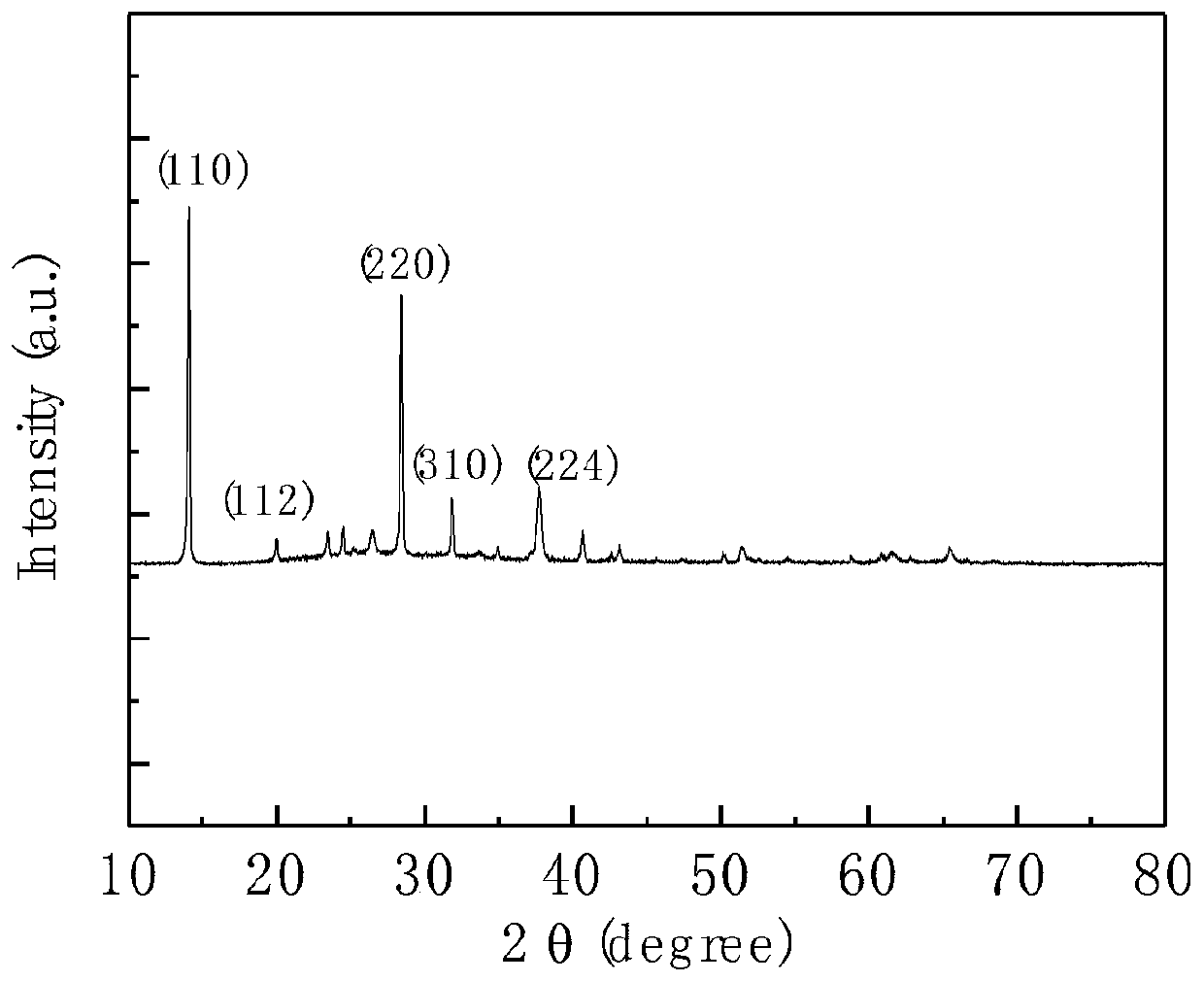
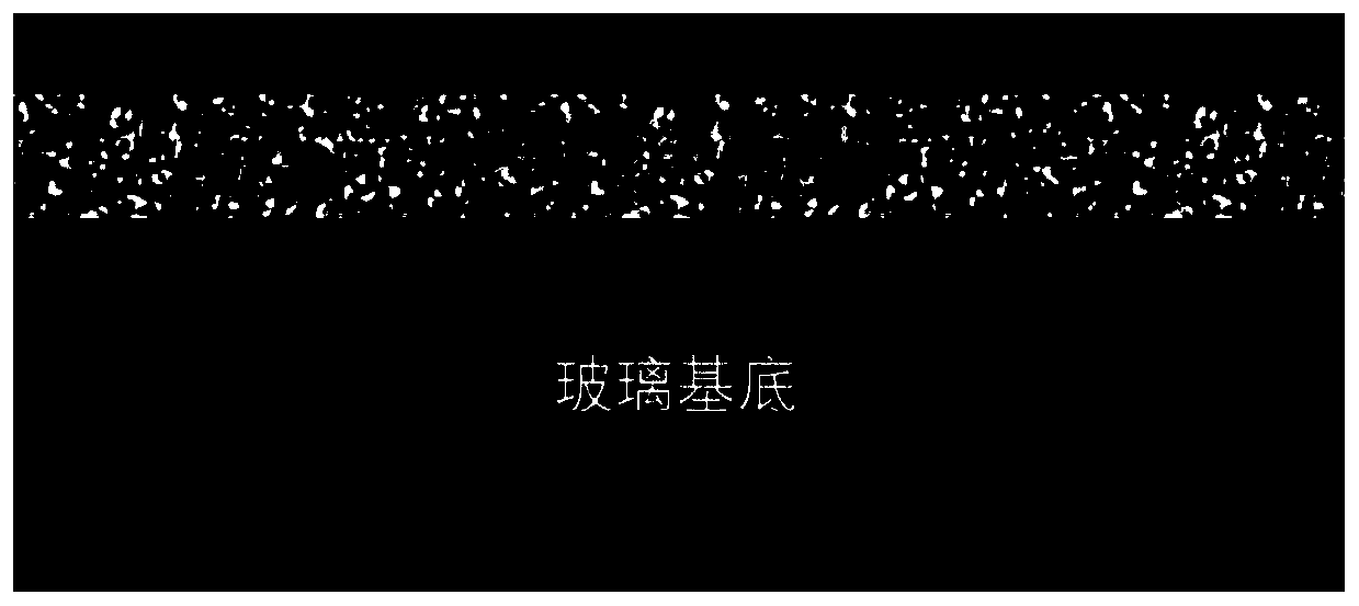
[0025] The schematic diagram of the passivation structure of a method for passivating perovskite materials in this embodiment is as follows figure 1 As shown, it includes from top to bottom: an amorphous perovskite passivation layer, a perovskite nanosphere crystal, and a glass substrate.

[0026] 1. Add 4g PbI 2 , 1 mL cyclohexane, 1 g CH 3 NH 3 1, 2mL isopropyl alcohol (IPA) forms mixed solution and dissolves at 30 ℃, is configured as the precursor solution of passivation layer;

[0027] 2. Take the glass substrate loaded with perovskite nanospheres and place it in a freeze dryer at -10°C for 10 minutes;

[0028] 3. Take out the substrate, and spin-coat 400 μL of the passivation layer precursor solution on the substrate at -5°C to form a 15nm film;

[0029] 4. Move the substrate to a 25°C environment and let it stand for 30 minutes;

[0030] 5. Place the substrate in a freeze dryer at 5°C for 15 minutes;

[0031] 6. Take out the substrate and spin-coat 400 μL of the pa...

Embodiment 2

[0036] The schematic diagram of the passivation structure of a method for passivating perovskite materials in this embodiment is as follows figure 2 As shown, it includes from top to bottom: an amorphous perovskite passivation layer, a perovskite polycrystalline film, and a glass substrate.

[0037] 1. Add 3g PbI 2 , 2mL cyclohexane, 1g CH 3 NH 3 1, 2mL IPA is formed in the mixed solution, dissolves at 30 ℃, is configured as the precursor solution of passivation layer;

[0038] 2. Take the glass substrate loaded with the perovskite polycrystalline film and place it in a freeze dryer at -15°C for 6 minutes;

[0039] 3. Take out the substrate, and spin-coat 200 μL of the passivation layer precursor solution on the substrate at -5°C to form a 10nm film;

[0040] 4. Move the substrate to a 30°C environment and let it stand for 30 minutes;

[0041] 5. Place the substrate in a freeze dryer at 5°C for 15 minutes;

[0042] 6. Take out the substrate and spin-coat 400 μL of the p...

Embodiment 3

[0047] The schematic diagram of the passivation structure of a method for passivating perovskite materials in this embodiment is as follows figure 2 As shown, it includes from top to bottom: an amorphous perovskite passivation layer, a perovskite polycrystalline film, and a glass substrate.

[0048] 1. Add 4g PbI 2 , 1 mL cyclohexane, 1 g CH 3 NH 3 1, 2mL IPA is formed in the mixed solution, dissolves at 30 ℃, is configured as the precursor solution of passivation layer;

[0049] 2. Take the glass substrate loaded with perovskite nanospheres and place it in a freeze dryer at -15°C for 20 minutes;

[0050] 3. Take out the substrate, and spin-coat 100 μL of the passivation layer precursor solution on the substrate at -5°C to form an 8nm film;

[0051] 4. Move the substrate to a 30°C environment and let it stand for 30 minutes;

[0052] 5. Place the substrate in a freeze dryer at 5°C for 15 minutes;

[0053] 6. Take out the substrate and spin-coat 400 μL of the passivation...


PUM

PropertyMeasurementUnit
Thicknessaaaaaaaaaa

Abstract

The invention provides a preparation method of a perovskite passivation layer, and belongs to the technical field of crystal material processing. Aiming at solving the problem that at present, the heterogeneous passivation effect is not ideal, the perovskite homogeneous passivation technology is proposed. The crystallization kinetics process of a passivation layer precursor solution on the surfaceof a perovskite material is adjusted by controlling the temperature, an amorphous passivation layer is promoted to grow, the amorphous passivation layer is used for passivating the defects on the surface and grain boundary of the perovskite material, and the quality of the material is improved. The passivation method provided by the invention is simple in process and easy to implement, the thickness of the passivation layer can be flexibly controlled, the quality of the perovskite material is effectively improved, and the prepared perovskite material has the characteristics of low defect state density and good electrical properties. The method can be widely applied to photoelectronic devices such as light emitting diodes, transistors, field effect transistors, solar cells and lasers.

Description

technical field [0001] The invention belongs to the technical field of crystal material processing, and in particular relates to a method for improving the performance of perovskite materials. Background technique [0002] In recent years, metal halide perovskite materials have attracted much attention due to their suitable band gap, high optical absorption coefficient, high molar extinction coefficient, low exciton binding energy, and excellent carrier bipolar diffusion characteristics. Widespread concern. The material has broad application prospects in optoelectronic functional devices such as photovoltaics, field effect transistors, photodetectors, and spin devices. [0003] The photoelectric properties and stability of perovskite materials largely depend on the structural state at the surface and grain boundaries. Studies have shown that there are a large number of uncoordinated dangling bond defects on the surface and grain boundaries of the initially prepared perovsk...

Claims


Application Information

Patent Timeline
IPC IPC(8): H01L51/44H01L51/48
CPCH10K71/12H10K30/88Y02E10/549
Inventor 王奉友范琳孙云飞杨丽丽杨景海
Owner JILIN NORMAL UNIV
Learn More