Two-dimensional material heterojunction back gate negative capacitance tunneling transistor and preparation method thereof

A two-dimensional material and heterojunction technology, which is applied in the field of two-dimensional material heterojunction back-gate negative capacitance tunneling transistor and its preparation, can solve the problem of low on-state current, reduce off-state current and increase on-state current , to solve the effect of low open current

Inactive Publication Date: 2020-01-03
NORTHWESTERN POLYTECHNICAL UNIV
View PDF7 Cites 6 Cited by
  • Summary
  • Abstract
  • Description
  • Claims
  • Application Information

AI Technical Summary

Problems solved by technology

[0006] Adding ferroelectric materials to the traditional TFET gate dielectric can take advantage of the high on-state current of ...

Method used


Image

  • Two-dimensional material heterojunction back gate negative capacitance tunneling transistor and preparation method thereof
  • Two-dimensional material heterojunction back gate negative capacitance tunneling transistor and preparation method thereof
  • Two-dimensional material heterojunction back gate negative capacitance tunneling transistor and preparation method thereof

Examples


preparation example Construction

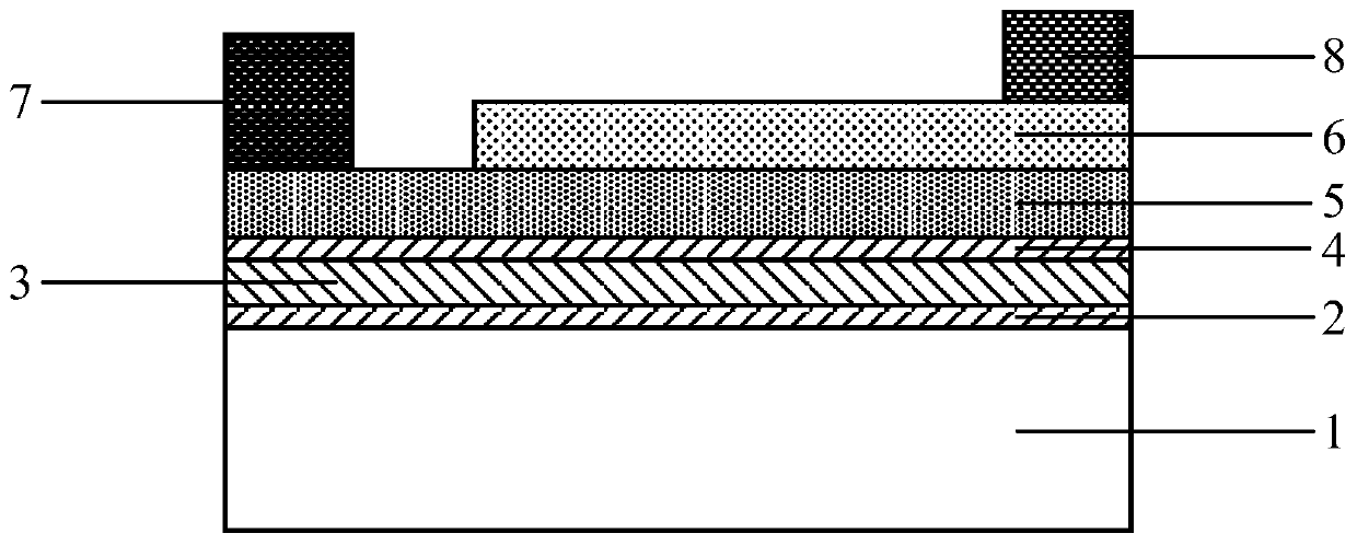
[0044] 2. Embodiment 1: refer to Figure 2 to Figure 9 , a method for preparing a two-dimensional material heterojunction back-gate negative capacitance tunneling transistor, comprising the following steps:

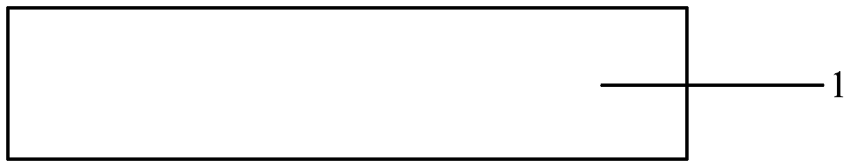
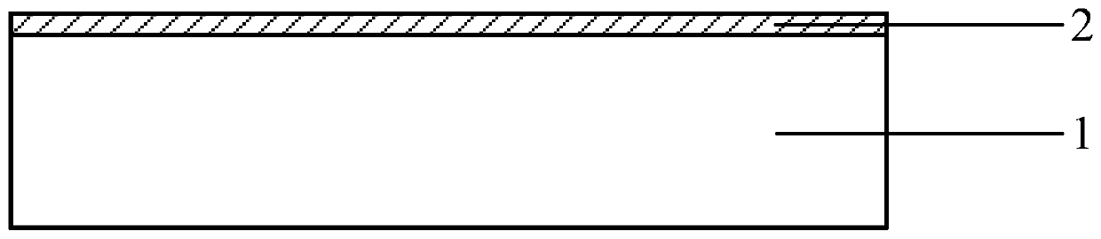
[0045] Step 1: Select a P-type Si substrate with a diameter of 2 inches and a crystal orientation of (100), and the doping concentration of the substrate is 1×10 18 / cm 3 , The resistivity is 0.1~0.5Ω·cm. In order to remove the natural oxides and impurities on the surface of the substrate, the substrate needs to be cleaned. The specific steps are as follows:

[0046] (1) Put the Si substrate into an acetone solution and ultrasonically clean it for 5 minutes, put the acetone-cleaned substrate into an ethanol solution and ultrasonically clean it for 5 minutes, and finally rinse it with deionized water for 1 minute to remove the Si substrate organic matter on the bottom;

[0047] (2) Clean the Si substrate in a mixed solution of hydrochloric acid, hydrogen peroxide, and ...

Embodiment 2

[0086] Embodiment 2: refer to Figure 2 to Figure 9 , a method for preparing a two-dimensional material heterojunction back-gate negative capacitance tunneling transistor, comprising the following steps:

[0087] Step 1: Select a P-type Si substrate with a diameter of 2 inches and a crystal orientation of (100), and the doping concentration of the substrate is 1×10 18 / cm 3 , The resistivity is 0.1~0.5Ω·cm. In order to remove the natural oxides and impurities on the surface of the substrate, the substrate needs to be cleaned. The specific steps are as follows:

[0088] (1) Put the Si substrate into an acetone solution and ultrasonically clean it for 5 minutes, put the acetone-cleaned substrate into an ethanol solution and ultrasonically clean it for 5 minutes, and finally rinse it with deionized water for 1 minute to remove the Si substrate organic matter on the bottom;

[0089] (2) Clean the Si substrate in a mixed solution of hydrochloric acid, hydrogen peroxide, and dei...


PUM

PropertyMeasurementUnit
Thicknessaaaaaaaaaa
Thicknessaaaaaaaaaa
Thicknessaaaaaaaaaa

Abstract

The invention relates to the technical field of semiconductor devices, and particularly discloses a two-dimensional material heterojunction back gate negative capacitance tunneling transistor. The transistor comprises a semiconductor substrate (1), a first high-k dielectric layer (2), a ferroelectric material layer (3), a second high-k dielectric layer (4), a first two-dimensional material layer (5), a second two-dimensional material layer (6), a metal source electrode (7) and a metal drain electrode (8). The advantages of the negative capacitance and the two-dimensional material are brought into full play, the on-state current of the tunneling field effect transistor is improved, and the off-state current of the tunneling field effect transistor is reduced. A preparation method of the two-dimensional material heterojunction back gate negative capacitance tunneling transistor is also disclosed, which comprises the growth of all the material layers. Because of the adoption of aback gatestructure, the device is simple in preparation process and compatible with a traditional semiconductor process.

Description

technical field [0001] The invention belongs to the technical field of semiconductor devices, and in particular relates to a two-dimensional material heterojunction back-gate negative capacitance tunneling transistor and a preparation method thereof. Background technique [0002] With the reduction in the size of semiconductor devices, traditional MOSFETs (metal-oxide semiconductor field-effect transistors) have encountered a series of problems caused by small size effects: although the gate length of MOSFETs continues to decrease, their operating voltage cannot continue to decrease. This makes power consumption a major challenge for MOSFETs, because the working mechanism of MOSFET thermal electron emission makes the sub-threshold swing unable to be lower than 60mV / dec; when the gate length of MOSFET is reduced, the limitation of the minimum sub-threshold swing makes MOSFET The off-state current increases, and the higher off-state current of MOSFET is the main source of its ...

Claims


Application Information

Patent Timeline
IPC IPC(8): H01L29/739H01L29/267H01L29/47H01L29/49H01L29/51H01L21/331
CPCH01L29/267H01L29/47H01L29/4916H01L29/516H01L29/66356H01L29/7391
Inventor 李伟汪钰成关赫汪瑛
Owner NORTHWESTERN POLYTECHNICAL UNIV
Why Eureka
Try Eureka